The pursuit of reliable electrical conductivity in nanocrystal quantum dot solids has long presented a challenge, hindering progress in areas like solar energy and advanced electronics. Xiangxi Yin, Bence Papp, and Shane Revel, from the University of California Riverside, alongside Sk Tahmid Shahriar and Tamar S. Mentzel, now report a significant advance in understanding how charge moves through these materials. The team developed a novel nano-patterning technique to create a highly ordered quantum dot solid, minimising structural defects and allowing them to isolate the behaviour of individual charge pathways. Their measurements reveal unexpectedly high levels of conductance noise, exceeding the average current, and demonstrate complex dynamics including random fluctuations and stable transport states, which they model using a quasi-one-dimensional percolation approach. This detailed insight into charge transport, unimpeded by material imperfections, paves the way for designing quantum dot solids with precisely tailored electrical properties and unlocks their potential for next-generation electronic devices.
The bottom-up assembly of designer solids represents a significant area of research. Quantum dot solids have already achieved considerable success in applications exploiting their tunable optical properties, including LED displays, lighting, and bioimaging. However, applications dependent on electrical properties, such as solar cells, photodetectors, and transistors, have not fully realised their potential due to limitations in controlling these properties. Furthermore, promising areas like solid-state quantum simulators for quantum computation and spintronics remain stagnant, largely because of a lack of clarity regarding the underlying charge transport mechanisms.
PbS Quantum Dot Array Disorder and Transport
This research investigates charge transport and the role of defects in colloidal quantum dot (QD) arrays, specifically lead sulfide (PbS) QDs. The central finding is that charge transport in these QD arrays is not simple band-like conduction, but is heavily influenced by disorder and the presence of localized states, or traps. This leads to anomalous transport behavior, deviating from standard models of conductivity. Researchers used techniques like photocurrent transient spectroscopy and advanced microscopy to characterize these trap states, finding that their density and distribution are crucial in determining the overall conductivity.
The observed charge transport does not follow Ohm’s Law or the Drude model, instead exhibiting characteristics like non-linear current-voltage relationships and deviations from standard diffusion. The team proposes that Lévy statistics, a type of statistical distribution describing random events with large fluctuations, can explain the observed transport characteristics, suggesting a hopping mechanism where charge carriers move between localized states. The system exhibits non-ergodic behavior, meaning its statistical properties change over time, linked to the presence of traps and the slow rearrangement of charge carriers. The team draws parallels between the observed transport in QD arrays and other disordered systems, such as amorphous semiconductors and glassy materials, suggesting similar underlying physics.
They highlight the importance of surface chemistry and passivation, coating the QDs to reduce surface defects, in controlling the density of trap states. Proper passivation can reduce the number of traps and improve charge transport. The findings have important implications for the development of QD-based electronic devices, such as solar cells, transistors, and photodetectors. Understanding the role of disorder and trap states is crucial for optimizing device performance. Future research will focus on developing new passivation techniques to further reduce trap density, exploring different QD materials and architectures to improve charge transport, developing more sophisticated models to accurately describe the complex transport phenomena, and investigating the potential of using Lévy statistics to design new types of electronic devices.
Conductance Noise Dominates Nanocrystal Charge Transport
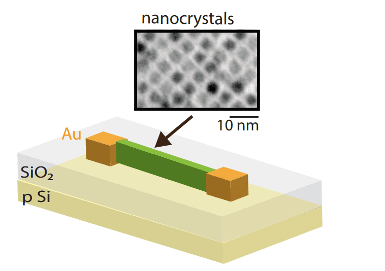
Scientists have achieved a breakthrough in understanding charge transport within colloidal nanocrystal solids, fabricating a 70-nanometer wide material free from many structural defects. This precise nano-patterning allows isolation of charge dynamics within a single conductance channel in a percolation network, enabling detailed measurement of electrical properties. Experiments reveal that conductance noise exceeds 100% of the average current, demonstrating significant fluctuations in charge flow. Detailed time-resolved measurements show that the current varies linearly with the standard deviation, confirming this is conductance noise, a variation in the channel’s ability to conduct electricity.
The average current and noise both increase exponentially with applied voltage, consistent with charge transport via tunneling through potential barriers created by surface ligands. Analysis of the noise spectrum reveals a power law dependence, ruling out common noise sources like white noise or pink noise. The team modeled the solid as a network of approximately ten nanocrystals wide and four high, proposing that charge transport occurs via majority hole carriers tunneling between nanocrystals. Disorder in the energy landscape, including variations in nanocrystal spacing and size, contributes to fluctuations in hopping rates.
They demonstrate that the solid behaves as a percolation network, where current is dominated by the lowest resistance paths, and trap states within these paths can significantly alter conductance. Further measurements of time-dependent current reveal a random telegraph signal, consistent with a single conductance channel fluctuating between on and off states due to nearby trap states. Histograms of off-times fit a power law with a long tail, indicating a wide distribution of trapping times and trap depths. This work provides a path toward rational design of nanocrystal solids with tailored electrical properties, opening possibilities for advanced electronic devices.
Phonon-Assisted Tunneling in Nanocrystal Solids
This research delivers significant advances in understanding charge transport within colloidal nanocrystal solids, materials with potential applications in advanced optoelectronics. By developing a novel nano-patterning technique, scientists fabricated a highly ordered nanocrystal solid, minimizing structural defects such as clustering, cracking, and grain boundaries. This enabled the isolation and direct observation of charge dynamics within a single conducting channel, revealing that transport is governed by phonon-assisted tunneling between nanocrystals, dynamically modulated by charge trapping events. The team characterized the observed charge transport using a stochastic model based on quasi-one-dimensional percolation paths, demonstrating that the system adheres to the ergodic hypothesis and behaves as a stationary system.
Analysis of long-time dynamics revealed a Lévy distribution in intermediate times, transitioning to deterministic behavior over extended periods. While acknowledging remaining sources of disorder, variations in nanocrystal site energy, tunneling coupling, and charge trapping, the researchers propose that enhanced coupling between nanocrystals and improved passivation of trap states can further refine control over electrical properties. This work establishes a clear pathway toward realizing designer nanocrystal solids with predictable and tunable electrical characteristics. Future efforts will focus on addressing the remaining sources of disorder and validating improvements through synthesis and fabrication, ultimately unlocking the full potential of nanocrystal solids for advanced optoelectronic devices and investigations into fundamental charge and spin properties.
👉 More information
🗞 Charge dynamics of individual conductance channels within a percolation network of a nano-patterned nanocrystal quantum dot solid
🧠 ArXiv: https://arxiv.org/abs/2510.01162


