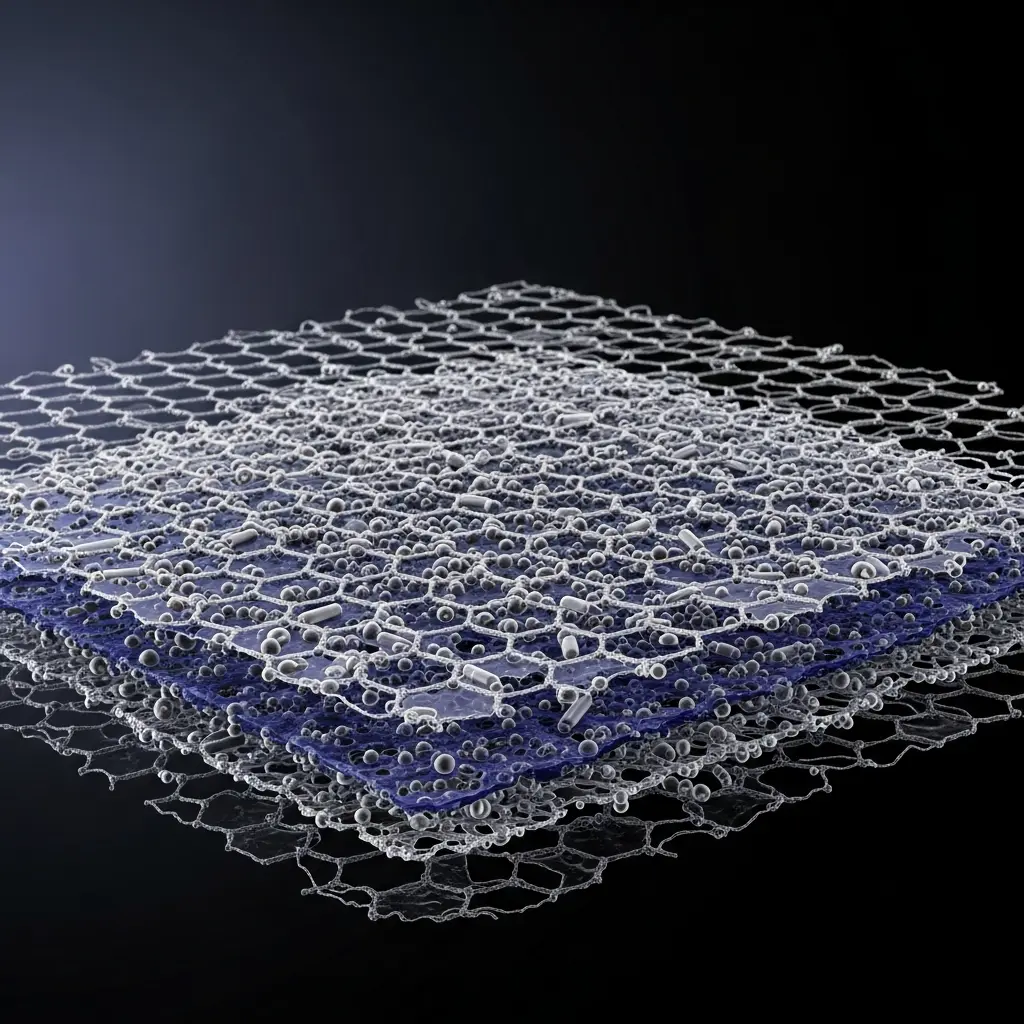
Researchers have, for decades, sought to observe the quantum Hall effect at ever lower magnetic fields, pushing the boundaries of condensed matter physics. Alexander S. Mayorov, Ping Wang, and Xiaokai Yue, from the National Laboratory of Solid State Microstructures and Sichuan Normal University, alongside colleagues Wu, He, Zhang et al, report a breakthrough in achieving this goal, observing integer quantum Hall features at an astonishingly low field of just 0.002 Tesla. Their work demonstrates a novel double-layer heterostructure design , utilising ultra-thin hexagonal boron nitride , which significantly reduces sample inhomogeneity and boosts carrier mobility, allowing access to the low-density regimes where quantum phenomena truly flourish. This advance not only facilitates the investigation of fundamental electronic interactions and strongly correlated phases, but also paves the way for future device applications reliant on precise carrier control and enhanced performance.
This discovery is particularly significant as it demonstrates the potential for exploring exotic quantum phenomena in graphene-based systems under readily achievable experimental conditions. This mutual screening significantly reduces the impact of charge impurities, which typically cause electron-hole puddles and limit carrier mobility near the charge neutrality point.
Two distinct types of ohmic contacts, Type I and Type II, were implemented to further refine device performance and minimise disorder, Type II contacts utilising a thick graphite layer to avoid issues associated with metal deposition and work function mismatches. The resulting platform not only enhances fundamental understanding of two-dimensional electronic systems but also opens exciting avenues for developing advanced electronic devices with superior performance characteristics. This research establishes a new standard for graphene heterostructure fabrication, offering a pathway towards realising the full potential of graphene in practical applications. This work opens up possibilities for creating more energy-efficient and high-performance electronic devices based on graphene and other two-dimensional materials.
Double-layer graphene heterostructure fabrication and mobility enhancement
The team meticulously fabricated these heterostructures, focusing on achieving a precise layer separation to maximise the screening effect and improve overall device performance. To quantify the enhancement, researchers calculated the ratio of mobilities between the double- and single-layer structures, revealing values as high as 3 to 4, aligning with observed high mobilities in their samples. This calculation considered the intralayer and interlayer Coulomb interactions, modelled as ǀ11 = ǀ22 = 2lj2/Ǖ and ǀ12 = ǀ21 = 2lj2/ Ǖ lj−ǕLj, where 1 and 2 denote the layers and Ǖ represents the transfer momentum. The study pioneered a method for determining total carrier density (tot) and displacement field (Ʈ) using the equation tot = ƭbgǀbg + ƭtgǀtg /lj −0 and Ʈ = ƭbgǀbg −ƭtgǀtg / 20 −Ʈ0, where ƭtg and ƭbg are the top and bottom gate capacitances per unit area. Transverse resistance measurements in tot −Ʈ space clearly demonstrated plateau-like structures indicative of QHE, conducted at Ƭ = 5 mT and ƾ = 20 mK. Longitudinal and Hall resistance were measured as a function of magnetic field and total concentration, revealing plateaus at total filling factors of -4 and +4 appearing at 2 mT, signifying the onset of the QHE for device D5.
Ultra-low field quantum Hall effect observed in graphene
The team meticulously fabricated several devices, DG2, each with varying widths and contact types to optimise performance. Two distinct ohmic contact types, Type I and Type II, were implemented and tested; Type II contacts, utilising a thick graphite layer, successfully avoided disorder introduced during metal deposition and work function disparities. Measurements on device D2, with a 5.5μm channel width, were compared to those from device D1, which had a 1.5 −2μm channel width, to assess the impact of channel dimensions on device characteristics. The resistivity of the fabricated devices reached a minimum value, indicating optimal carrier transport properties.
The research team observed that even when both graphene layers were near the charge neutrality point, the mutual screening effect markedly enhanced charge carrier uniformity. This enhancement arises because the second graphene layer shields electric fields from impurities, limiting their impact to a single layer and preventing scattering of charge carriers in the opposing layer. Measurements confirm that this double-layer graphene system (DLG) exhibits Hall edge states, typically observed under strong perpendicular magnetic fields. These results demonstrate the potential for precise carrier-density control via gating, making this architecture an ideal platform for studying electronic interactions.
High-mobility graphene heterostructures and low-field oscillations offer promising
Scientists have demonstrated a significant advancement in the fabrication of high-mobility graphene heterostructures, achieving unprecedented control over carrier density and opening new avenues for exploring fundamental electronic phenomena. The authors acknowledge that boundary scattering becomes increasingly dominant as bulk disorder is reduced, directly linking mobility to channel width, a limitation for certain device geometries. Future research could focus on optimising channel dimensions to mitigate this effect and further enhance performance. These findings represent a substantial step forward in materials science, providing a robust platform for fundamental studies of quantum phenomena and potentially enabling the development of advanced electronic devices based on graphene heterostructures.
👉 More information
🗞 Quantum Hall Effect at 0.002T
🧠 ArXiv: https://arxiv.org/abs/2601.16015


