Trapped ions represent a leading technology in the quest to build powerful quantum computers, but scaling these systems to the large number of qubits needed for complex calculations presents significant engineering challenges. Bassem Badawi, Philip C. Holz, Michael Raffetseder, and colleagues at the University of Innsbruck and the Fraunhofer Institute for Silicon Technology ISIT, alongside collaborators at Alpine Quantum Technologies GmbH, now demonstrate a novel approach to overcome these hurdles using chiplet technology. This modular design breaks away from traditional monolithic fabrication, instead creating separate processor modules, or chiplets, each optimised for a specific function. The team successfully built and tested a chiplet-based system for individually addressing ions within a ten-ion crystal, combining glass substrates for ion trapping with silicon-based waveguides and 3D-printed micro-optics, and this work paves the way for more flexible, scalable, and cost-effective quantum processors.
Investigations focus on core components like ion traps, exploring various designs including microfabricated traps for dense packing, multilayer traps for improved control, and 3D-printed traps offering design freedom. Ball-grid array architectures connect these microfabricated traps, enabling larger systems, while atomic ovens provide a compact and integrated approach to generating and loading ions. Maintaining stable ion confinement and manipulating their quantum states requires precise laser and radio frequency control, alongside ultra-high vacuum systems to minimize disturbances.
Scaling these systems involves modular architectures, connecting multiple trap modules to increase qubit count. A key focus is photonic interconnects, utilizing photons to entangle ions across different modules, with silicon photonics and other dielectric platforms like the triplex platform being actively explored. Waveguide structures guide light for entanglement, while research also investigates physically shuttling ions between trap zones to enable interactions. Significant challenges exist in materials science and engineering. Dielectric materials near ions can cause heating and decoherence, necessitating the development of low-loss dielectrics and anti-reflective coatings.
Surface treatments minimize unwanted effects, while thermal management techniques remove heat generated by lasers and electronics, and matching thermal expansion coefficients of different materials is crucial for maintaining alignment. Preventing charge buildup on surfaces and utilizing transparent traps to allow light access are also key considerations. Accurate state detection is essential, relying on single-photon detectors like avalanche photodiodes and superconducting nanowire detectors. Researchers are exploring trap-integrated detectors for improved performance, alongside efficient fluorescence collection and alternative detection methods like photomultiplier tubes.
Microfabrication, 3D printing, laser-induced etching, and wafer bonding are employed to create these complex structures. Integration remains paramount, requiring careful materials selection, fabrication techniques, and design optimization. Photonics is the key to scaling, and materials science is critical for minimizing performance-limiting factors. This strategy addresses the increasing complexity of integrating diverse features, electrical routing, materials for heat dissipation, integrated optics, detectors, and stable trapping potentials into a single processor. By fabricating individual processor modules separately, the team can select optimal materials and fabrication technologies for each, minimizing limitations inherent in monolithic designs. This research demonstrates this chiplet approach with an integrated individual-ion addressing system for a ten-ion crystal.
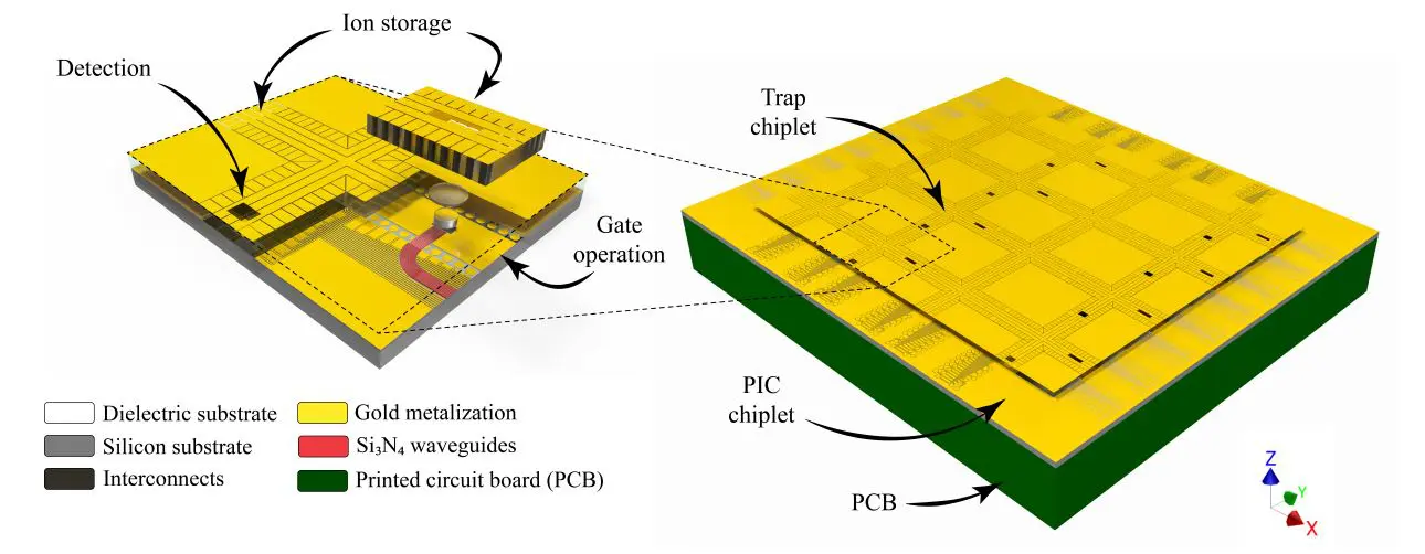
The system combines a surface ion trap manufactured on a glass substrate with a silicon substrate carrying integrated waveguides and 3D-printed micro-optics. Precise alignment of these components achieves diffraction-limited focal spots at each ion position, crucial for individual control and manipulation. This modular design simplifies fabrication by allowing the ion trap to be built on glass, minimizing radio frequency and photon absorption, while leveraging silicon for established optical waveguide platforms and CMOS technologies. Heterogeneous integration technology interfaces these bare ion trap chips with separately fabricated silicon chips, incorporating standard optical waveguide platforms, photon detection systems, cryogenic amplifiers, and digital-to-analog converters. Successful demonstration of a functional ion addressing system paves the way for more complex and scalable trapped-ion quantum computers. This work introduces a system where individual processor components, termed chiplets, are fabricated separately and then combined, enabling the selection of optimal materials and fabrication techniques for each function. The resulting system-in-package (SiP) architecture offers substantial advantages over conventional methods, particularly in terms of flexibility and cost-effectiveness. The team designed a SiP stack with a top layer dedicated to the ion trap chiplet, constructed from a dielectric material with low radio frequency (RF) loss to minimize signal absorption.
This chiplet features electrodes for ion trapping and through-substrate vias for electrical connections, alongside openings for integrating microfabricated optical elements. A second layer incorporates supply chiplets for routing photonic and electric signals, providing control over the quantum system. This modular construction allows for independent revision or modification of individual components without impacting the entire processor, significantly accelerating development cycles. Experiments demonstrate the feasibility of this approach, showcasing an integrated individual-ion addressing system for a ten-ion crystal.
The design emphasizes the benefits of heterogeneous integration, combining a glass substrate for the surface ion trap with a silicon substrate carrying integrated waveguides. This combination delivers diffraction-limited focal spots at the ion positions, crucial for precise control and manipulation of individual qubits. The chiplet approach allows for the fusion of multiple manufacturing technologies and materials, selecting the best technology for each functionality within the processor. This modularity promises faster, more cost-efficient development and increased reliability compared to monolithic designs, paving the way for scalable trapped-ion quantum computing.
Modular Trapped-Ion Processor with Integrated Laser Control
This work demonstrates a new modular approach to building trapped-ion quantum processors, moving beyond traditional monolithic fabrication techniques. Researchers have successfully designed and fabricated a processor based on ‘chiplets’, small, independently manufactured modules with specific functions, that are then integrated to form a complete system. This strategy allows for the selection of optimal materials and fabrication processes for each chiplet, offering greater flexibility and potentially reducing manufacturing limitations compared to creating a single, complex component. The team realized a proof-of-concept processor with an integrated laser-addressing system capable of individually controlling ten ions within a crystal.
This system combines a glass-based ion trap chiplet with a silicon chiplet containing optical waveguides, connected via gold bonding. Crucially, the researchers achieved diffraction-limited focusing of laser beams onto the ion positions, demonstrating the precision required for quantum operations. They also confirmed successful bonding between the chiplets, mitigating stress caused by material differences. While this chiplet approach simplifies the fabrication of individual components, it introduces complexity in the packaging and integration stages. Future work will focus on refining these integration techniques and establishing robust interfaces between chiplets. This modular design, however, promises faster development cycles and cost-effective upgrades, paving the way for more complex and scalable trapped-ion quantum computers.
🗞 Chiplet technology for large-scale trapped-ion quantum processors
🧠 ArXiv: https://arxiv.org/abs/2512.02645


