Understanding the behaviour of light within semiconductor structures is crucial for developing advanced technologies in the mid-infrared, and researchers are continually striving for more accurate predictive models. Konstantinos Pantzas, Virginie Trinité, and Angel Vasanelli, alongside Carlo Sirtori, Grégoire Beaudoin, and Isabelle Sagnes, have achieved a significant step forward in this area by developing a highly accurate method for predicting optical transitions within complex InGaAs/InAlAs semiconductor structures. The team’s approach involves detailed modelling of the material composition, accounting for subtle variations at the interfaces between different layers, and this allows them to simulate light absorption with unprecedented precision, improving upon previous methods by almost tenfold. This breakthrough promises to accelerate the design and optimisation of high-performance devices for emission, modulation, and detection in the mid-infrared spectrum.
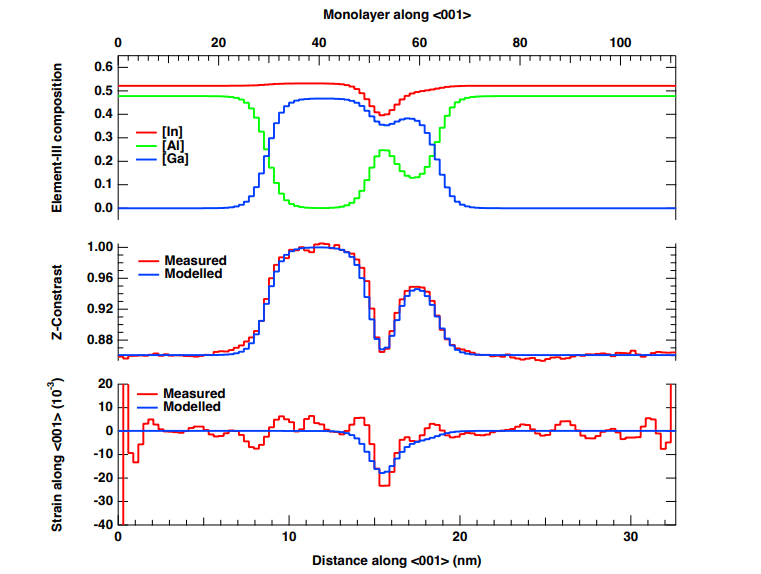
Atomically-resolved Z-contrast and strain mappings provide a detailed model of the composition of an InGaAs/InAlAs asymmetric coupled quantum-well structure grown on InP using metal-organic vapor phase epitaxy. This model accounts for compositional variations across multiple alloy interfaces, a critical factor often neglected in simpler simulations.
Compositional Grading in Complex Quantum Well Structures
Scientists developed a comprehensive model to accurately determine the composition of complex InGaAs/InAlAs asymmetric coupled quantum-well structures grown on InP substrates using metal-organic vapor phase epitaxy. This work addresses the challenge of accurately predicting the optical properties of these heterostructures, crucial for mid-infrared emission, modulation, and detection technologies. The model accounts for compositional grading across multiple alloy interfaces, a critical factor often overlooked in simpler simulations, and provides a versatile framework for analyzing complex material designs. To calibrate and validate the model, the team grew a specific asymmetric coupled quantum-well structure, consisting of 5.
6nm and 2. 5nm thick InGaAs wells separated by a 1. 4nm InAlAs barrier, surrounded by 25nm thick InAlAs barriers, using a Veeco D180 Turbodisc MOVPE reactor. Trimethylgallium, trimethylaluminum, trimethylindium, and arsine served as precursors for gallium, aluminum, indium, and arsenic, ensuring lattice matching with the InP substrate. A key innovation involved employing an aluminum flow modulation scheme during the growth of the thin InAlAs barrier, compensating for aluminum loss and improving barrier quality.
Detailed compositional and strain mapping was achieved using aberration-corrected scanning transmission electron microscopy, specifically with a FEI 4 TITAN 200 TEM-STEM operating at 200 keV. The team utilized a probe convergence half-angle of 17. 6 mrad and detection angles of 69 mrad and 200 mrad to obtain atomically-resolved images along the ⟨1 1 0⟩ zone axis. These high-resolution images were then analyzed using a specialized algorithm to quantify the composition and strain within the structure, providing experimental data for model calibration. Furthermore, a separate sample containing thirty repetitions of the ACQW structure was grown with an n-doped 5.
6nm InGaAs well, targeting a concentration of 1. 5 × 1018cm−3, and a semi-insulating InP substrate to minimize free-carrier absorption. Absorption measurements were performed using a Fourier-Transform Infrared spectrometer and a multi-pass absorption cavity, allowing for precise determination of the structure’s optical properties. The sample was positioned at Brewster angle within a dry nitrogen atmosphere, and light from a globar source, filtered with a linear TM polarizer, was used to probe the absorption spectrum.
Alloy Composition Impacts Quantum Well Spectra
Scientists achieved a tenfold improvement in the accuracy of simulating the absorption spectrum of an InGaAs/InAlAs asymmetric coupled quantum-well structure, grown on InP, by developing a detailed model of alloy composition across multiple interfaces. The research team used atomically-resolved Z-contrast imaging to map strain and composition, revealing significant deviations from nominal alloy compositions previously assumed in simulations. Specifically, the 1. 4nm thick InAlAs barrier contained at most 25% aluminum, 35% gallium, and 40% indium, while the subsequent 2. 4nm thick InGaAs well contained up to 10% aluminum.
The team modeled composition profiles and computed band structures, demonstrating that the actual structure’s energy levels differed significantly from those predicted by a square-band potential model. Level E3, in particular, was distributed across the entire width of the structure in the actual model, whereas it was localized within the well in the square-band equivalent. These differences yielded a substantial impact on the absorption spectra, with the peak absorption for the E12 transition appearing at 170 meV in the experimental spectrum. The sigmoidal profile accurately reproduced this peak, while the square-band equivalent was offset at 144 meV, representing a 1.
4μm shift in the operating wavelength. Furthermore, the team accurately predicted the E13 transition at 278 meV, closely matching the experimental peak of 281 meV, compared to 272 meV for the square-band model. This level of precision is crucial for designing unipolar devices operating in the mid-infrared, and the researchers have already utilized this information to create a Stark-effect modulator achieving a record 10 Gbps free-space communication channel at 9μm.
Accurate Superlattice Modelling Predicts Absorption Spectra
Researchers have developed a generalized empirical model for epitaxial semiconductor superlattices, accurately capturing the complex composition of these structures at the atomic level. By employing atomically-resolved imaging and strain mapping, the team successfully accounted for compositional grading across multiple alloy interfaces, a feature often overlooked in simpler models. This refined model accurately predicts the intersubband absorption spectrum of an asymmetric coupled quantum-well structure, achieving a ten-fold improvement in accuracy compared to simulations relying on nominal alloy compositions. Accurate modelling is crucial for optimising the performance of these materials in applications such as emission, modulation, and detection technologies. The authors acknowledge that the model could be further refined by incorporating precursor flow ratios during growth and by analysing the distribution of elements within single atomic monolayers to more precisely predict optical transition linewidths. Future work may focus on these areas to further enhance the model’s predictive capabilities and broaden its applicability to a wider range of semiconductor superlattice structures.
👉 More information
🗞 Accurate prediction of optical transitions in epitaxial InGaAs/InAlAs asymmetric coupled quantum well structures
🧠 ArXiv: https://arxiv.org/abs/2509.19951


