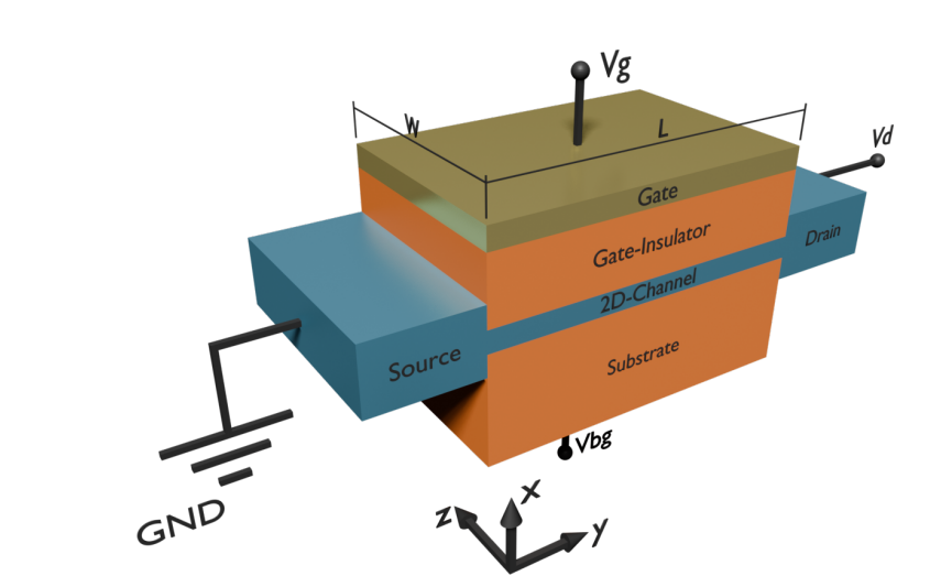
Hysteresis, a lagging of a material’s response to changing conditions, frequently appears in transistors built from two-dimensional materials, yet its significance remains poorly understood. Alexander Karl, Dominic Waldhoer, and Theresia Knobloch, alongside Axel Verdianu, Joël Kurzweil, Mina Bahrami, and colleagues, address this challenge with a systematic investigation into the origins of hysteresis in these devices. The team reveals that previously reported hysteresis values lack meaningful comparison due to inconsistent measurement conditions and a fragmented understanding of the underlying mechanisms, which include charge trapping, mobile charge drift, and, potentially, ferroelectricity. To resolve this, they propose a standardised measurement scheme that not only allows for accurate comparison of device stability across different materials, but also enables prediction of performance in future, ultra-thin designs, ultimately accelerating the development of more reliable 2D-material-based transistors.
Quantum Capacitance in Two-Dimensional Transistors
Research into two-dimensional materials like molybdenum disulfide and tungsten diselenide reveals the importance of quantum capacitance in nanoscale transistors. This non-classical capacitance, arising from the quantization of electron density, significantly impacts device behaviour and requires accurate modeling. Scientists are developing compact models for these 2D field-effect transistors, carefully accounting for charge distribution and capacitance within the device. Further investigations explore the properties of ferroelectric materials, such as hafnium oxide and strontium titanate, including their polarization switching and temperature dependence, integrating them into transistors to create novel memory devices and enhance performance. This research combines insights from semiconductor physics, materials science, and device modeling to advance the development of next-generation electronic devices.
Standardized Hysteresis Measurement in 2D-MOSFETs
Scientists have established a standardized method for accurately measuring and comparing hysteresis in transistors built from two-dimensional materials. Recognizing inconsistencies in previous measurements, the team conducted a thorough theoretical analysis of factors contributing to hysteresis, including charge trapping, mobile charge drift, and potential ferroelectric effects. This analysis guided the design of experiments to pinpoint the root causes of instability in emerging 2D-MOSFETs. The study introduces a precise measurement scheme employing a triangular staircase signal applied to the transistor’s gate, defined by minimum and maximum voltages and sweep frequency.
A small drain voltage minimizes electric field effects and simplifies analysis of channel characteristics. By recording drain current and plotting it against gate voltage, scientists quantify hysteresis width as the shift in threshold voltage between up- and down-sweeps. To ensure reliable data, the researchers tracked hysteresis evolution over multiple sweep cycles at a low frequency, allowing devices to reach a stable state. This approach isolates the intrinsic hysteresis value, providing a comparable metric for assessing device stability and benchmarking insulator/channel combinations. The standardized method also enables extrapolation of data to sub-nanometer equivalent oxide thicknesses, facilitating effective screening of materials for reliable 2D-MOSFETs.
Defect Dynamics Govern Hysteresis in 2D Transistors
Scientists have gained a comprehensive understanding of hysteresis in two-dimensional material-based transistors, establishing a standardized measurement scheme to assess device stability. The work addresses ambiguity in reported hysteresis values by detailing the underlying mechanisms and experimental factors influencing their measurement. Researchers theoretically analyzed charge trapping by defects, mobile charge drift, and the potential role of ferroelectricity, ultimately focusing on charge trapping and defect dynamics as dominant contributors. Experiments reveal that the equilibrium occupation of defects is governed by Fermi-Dirac statistics, meaning the defect’s charge state depends on its energy level relative to the channel’s Fermi level.
The team identified an “active energy region” near the channel and gate within the insulator, representing the area where defects can change their charge state and contribute to hysteresis. Simulations show that the channel-side active energy region is significantly larger than the gate-side region, indicating that defects closer to the channel have a greater impact on hysteresis. Measurements demonstrate that hysteresis width is frequency-dependent, decreasing as the measurement frequency increases, from approximately 71mV at 10³ Hz to significantly lower values at 10⁹ Hz. Furthermore, the team found that hysteresis width is temperature-dependent, with higher temperatures resulting in reduced hysteresis. Using bismuth oxy selenide/bismuth selenoxide/gold stacks, the team measured hysteresis curves, demonstrating the influence of defect parameters on device performance. These results establish a clear link between material properties and device stability, enabling systematic benchmarking of insulator/channel combinations for reliable transistor design.
Standardized Hysteresis Measurement And Mechanism Dissection
This research delivers a comprehensive analysis of hysteresis in transistors built from two-dimensional materials. The team investigated the primary causes of hysteresis, specifically charge trapping by defects, the movement of mobile charges, and the potential for ferroelectric behaviour within the device, demonstrating methods to distinguish between these mechanisms based on their unique physical signatures. The study reveals that previously reported hysteresis values lacked meaningful comparison due to inconsistent measurement conditions. To address this, the researchers proposed a standardized measurement scheme that accounts for the thickness of the insulating layer within the transistor, normalizing data using a metric called equivalent oxide thickness. This approach enables reliable comparison of devices with different insulator thicknesses and allows for the prediction of hysteresis in ultra-thin devices based on measurements from larger prototypes. These advancements establish hysteresis as a dependable indicator of device quality and stability, expected to accelerate the development of more reliable two-dimensional material-based transistors for future electronic applications.
🗞 Hysteresis Measurements as a Diagnostic Tool: A Systematic Approach for Stability Benchmarking and Performance Projection of 2D-Materials-Based MOSFETs
🧠 ArXiv: https://arxiv.org/abs/2509.21315


