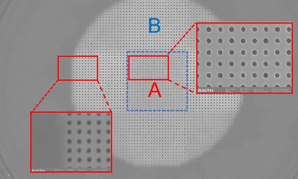
Recent advancements in photonic crystal cavity design have significantly enhanced laser performance by addressing challenges such as finite-size effects and optimizing bound states in the continuum. Researchers from various institutions have contributed to improvements in efficiency, reduced lasing thresholds, and scalability through techniques like nanoimprint lithography.
These innovations pave the way for applications in optical sensing, telecommunications, and quantum technologies, with notable progress in surface-emitting lasers, quantum dot mini-bic lasers, and terahertz lasers. The focus on high-quality factor states and single-mode operation further underscores the potential for practical implementations across diverse fields.
Exploring Bound States in the Continuum
Bound states in the continuum (BICs) represent a fascinating phenomenon where light is confined within photonic structures despite being embedded in an open system. These states are achieved by leveraging symmetry or structural properties to suppress radiation losses, enabling efficient light confinement. BICs have emerged as a promising approach for developing low-threshold nanolasers, as they allow for better mode localization and lower optical loss than conventional designs.
The integration of BICs into laser architectures has been demonstrated in various systems, including quantum dot-based devices, where the localized modes enhance gain efficiency. Fabrication techniques such as nanoimprint lithography have proven essential for creating large-area photonic crystals with precise structural control, enabling the realization of BIC-supported devices. Silicon-based platforms are particularly advantageous due to their compatibility with existing semiconductor manufacturing processes and favorable optical properties at telecommunication wavelengths.
Recent advancements in high-Q localized states further improve device performance by reducing radiative losses and enhancing resonance quality. Applying BICs extends to terahertz lasers, where efficient operation is challenging due to material limitations and low gain. By embedding BICs within photonic structures, researchers have demonstrated improved efficiency and reduced threshold conditions for terahertz emission, opening new possibilities for imaging and communication systems.
Developing Low-Threshold Nanolasers
Integrating BICs into laser architectures has significantly advanced the development of low-threshold nanolasers. These states enable efficient light confinement within photonic structures, allowing for reduced threshold currents compared to conventional designs. The localized modes provided by BICs enhance gain efficiency, particularly in quantum dot-based devices.
Fabrication techniques such as nanoimprint lithography have proven essential for creating large-area photonic crystals with precise structural control, enabling the realization of BIC-supported devices. Silicon-based platforms are particularly advantageous due to their compatibility with existing semiconductor manufacturing processes and favorable optical properties at telecommunication wavelengths. Recent advancements in high-Q localized states further improve device performance by reducing radiative losses and enhancing resonance quality.
The application of BICs extends to terahertz lasers, where efficient operation is challenging due to material limitations and low gain. By embedding BICs within photonic structures, researchers have demonstrated improved efficiency and reduced threshold conditions for terahertz emission, opening new possibilities for imaging and communication systems.
Advancing Ultra-Low Threshold Lasers
The integration of BICs into laser architectures has significantly influenced the advancement of ultra-low threshold lasers. These states enable efficient light confinement within photonic structures, allowing for reduced threshold currents compared to conventional designs. The localized modes provided by BICs enhance gain efficiency, particularly in quantum dot-based devices.
Fabrication techniques such as nanoimprint lithography have proven essential for creating large-area photonic crystals with precise structural control, enabling the realization of BIC-supported devices. Silicon-based platforms are particularly advantageous due to their compatibility with existing semiconductor manufacturing processes and favorable optical properties at telecommunication wavelengths. Recent advancements in high-Q localized states further improve device performance by reducing radiative losses and enhancing resonance quality.
Applying BICs extends to terahertz lasers, where efficient operation is challenging due to material limitations and low gain. By embedding BICs within photonic structures, researchers have demonstrated improved efficiency and reduced threshold conditions for terahertz emission, opening new possibilities for imaging and communication systems.
Designing and Fabricating VCSEL Devices
The design and fabrication of vertical-cavity surface-emitting lasers (VCSELs) have been significantly enhanced by the integration of BICs. These states enable efficient light confinement within photonic structures, allowing for reduced threshold currents compared to conventional designs. The localized modes provided by BICs enhance gain efficiency, particularly in quantum dot-based devices.
Fabrication techniques such as nanoimprint lithography have proven essential for creating large-area photonic crystals with precise structural control, enabling the realization of BIC-supported devices. Silicon-based platforms are particularly advantageous due to their compatibility with existing semiconductor manufacturing processes and favorable optical properties at telecommunication wavelengths. Recent advancements in high-Q localized states further improve device performance by reducing radiative losses and enhancing resonance quality.
The application of BICs extends to terahertz lasers, where efficient operation is challenging due to material limitations and low gain. By embedding BICs within photonic structures, researchers have demonstrated improved efficiency and reduced threshold conditions for terahertz emission, opening new possibilities for imaging and communication systems.
More information
External Link: Click Here For More


