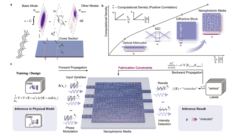
Researchers demonstrate an ultra-compact neural network, achieving 86.7% accuracy on the Iris dataset, utilising nanophotonic scattering and fabrication-aware inverse design. This on-chip architecture reduces the footprint by three orders of magnitude compared to conventional neural networks, promising energy-efficient and scalable AI inference.
The pursuit of increasingly compact and energy-efficient hardware is central to the continued development of artificial intelligence, particularly for deployment in resource-constrained environments. Researchers are now demonstrating significant reductions in the physical footprint of on-chip neural networks, a critical step towards scalable machine learning inference. A team led by Zhenyu Zhao, Yichen Pan, Jinlong Xiang, and colleagues from Shanghai Jiao Tong University, alongside Min Gu and Xinyuan Fang from the University of Shanghai for Science and Technology, detail their work in a recent publication entitled ‘High computational density nanophotonic media for machine learning inference’. Their approach utilises nanophotonic media and fabrication-aware inverse design to create an ultra-compact neural network architecture, achieving an area of just 64 μm² and an experimental accuracy of 86.7% on the Iris flower dataset, representing a substantial reduction in size compared to conventional systems.
Modern artificial intelligence increasingly demands substantial computational resources, yet faces limitations imposed by the physical scaling of traditional hardware and associated power consumption. Researchers continually investigate novel approaches to overcome these challenges, and a recent development demonstrates a nanophotonic machine learning system that substantially reduces device area while maintaining competitive accuracy. This novel system utilises silicon nanophotonics and fabrication-aware inverse design techniques, achieving a three-order-of-magnitude decrease in footprint compared to conventional on-chip neural networks, and potentially enabling more efficient and compact AI hardware.
The research addresses a critical need for denser
The research addresses a critical need for denser machine learning systems, as traditional electronic implementations struggle to keep pace with growing computational demands. Scientists fabricated ultra-compact neural networks, leveraging the unique properties of silicon nanophotonics to confine and control light at the nanoscale. Silicon nanophotonics utilises silicon as a medium for manipulating photons, offering advantages in miniaturisation and integration with existing microelectronic fabrication processes. Fabrication-aware inverse design played a crucial role, guiding the optimisation process to account for manufacturing constraints and ensure practical realisation of the complex nanophotonic structures. This approach allows for the creation of highly condensed systems, pushing the boundaries of integration and enabling new possibilities for edge computing and embedded AI applications.
Researchers evaluated the prototype’s performance using the Iris flower dataset, a standard benchmark for classification tasks, and obtained an accuracy of 86.7%, closely aligning with simulation predictions. Finite-Difference Time-Domain (FDTD) simulations, performed using Ansys Lumerical FDTD software and the NumPy Python package, modeled light propagation through the nanophotonic structures and facilitated gradient calculations essential for training the network. FDTD is a numerical technique used to solve Maxwell’s equations, which govern the behaviour of electromagnetic waves, allowing researchers to predict how light will interact with the nanophotonic structures. Both 3D and 2.5D FDTD methods proved valuable, adapting to the specific requirements of different tasks and optimising computational efficiency.
The research distinguishes itself through a strong focus on manufacturability, integrating fabrication constraints directly into the design process. This proactive approach ensures that the complex nanophotonic structures can be reliably fabricated using existing techniques, bridging the gap between theoretical designs and practical implementations. The resulting system exhibits low latency, measured at 0.11 picoseconds, and lowers power consumption, making it ideal for mobile and embedded applications.
This development represents a significant step forward in
This development represents a significant step forward in the pursuit of next-generation AI hardware, offering a compelling solution to reduce the hardware footprint, latency, and power consumption of future artificial intelligence applications. Further research will focus on scaling this technology, improving its accuracy, and exploring new applications, paving the way for a future where AI is more accessible, efficient, and sustainable.
Researchers plan to explore the incorporation of nonlinearity into the design, a promising avenue for enhancing performance and expanding the capabilities of the nanophotonic neural network. Investigating alternative datasets and machine learning algorithms will broaden the applicability of this approach, demonstrating its versatility and potential for solving a wider range of problems. Additionally, research into scalable fabrication techniques will be crucial for translating this technology from the laboratory to real-world applications, enabling mass production and widespread adoption.
The research receives funding from the National Key R&D Program of China, the Natural Science Foundation of China, and the Shanghai Municipal Science and Technology Major Project, demonstrating a commitment to advancing the field of artificial intelligence. Fabrication support provided by the Center for Advanced Electronic Materials and Devices (AEMD) at Shanghai Jiong University further strengthens the collaborative effort. The authors declare no conflicts of interest and make data available upon request, signifying a commitment to open scientific practice and fostering collaboration within the research community.
🗞 High computational density nanophotonic media for machine learning inference
🧠 DOI: https://doi.org/10.48550/arXiv.2506.14269


