The quest for increasingly miniaturised electronics drives research into novel diode designs, and a team led by Elias Eckmann, Ersoy Şaşıoğlu, and Nicki F. Hinsche at the Martin Luther University Halle-Wittenberg now presents a promising pathway using a single material, molybdenum disulphide. Their work demonstrates that carefully engineered junctions within this material, switching between semiconducting and metallic phases, can mimic the behaviour of traditional metal-insulator-metal diodes. This achievement overcomes a key limitation in nanoscale electronics, which often struggles with the complexities of joining dissimilar materials, and opens up possibilities for creating fully two-dimensional, in-plane diodes. The researchers reveal that this rectification arises from the creation of internal electrical steps at the interfaces between the different phases, establishing a built-in potential that governs current flow and paving the way for high-frequency detectors and energy-harvesting devices.
Phase-Engineered Rectification in Molybdenum Disulfide Homojunctions
Lateral two-dimensional tunnel diodes that reproduce metal-insulator-metal (MIM)-diode-like rectification without using dissimilar contacts are attractive for scalable nanoelectronics. Molybdenum disulfide can exist in both the metallic 1T phase and the semiconducting 1H phase, enabling phase-engineered homojunctions. This research investigates the formation of MIM-diode-like rectification in lateral 1T/1H/1T-molybdenum disulfide homojunctions through interfacial dipole engineering. The approach involves creating a lateral homojunction within a single molybdenum disulfide flake, transitioning from the metallic 1T phase to the semiconducting 1H phase and back to the metallic 1T phase.
By carefully controlling this phase transition, the team engineers an interfacial dipole at the 1T/1H and 1H/1T interfaces, crucial for achieving rectification. The results demonstrate that this engineered dipole effectively modulates charge carrier transport across the homojunction, leading to a pronounced MIM-diode-like current-voltage characteristic. This achievement provides a pathway towards fabricating compact, scalable, and low-power nanoelectronic devices based on a single material system, eliminating the need for complex heterojunction fabrication.
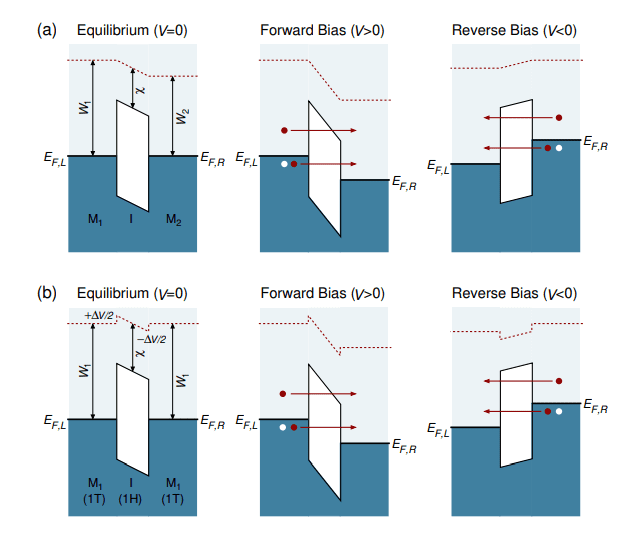
First-principles electronic structure and quantum transport calculations show that phase-engineered 1T/1H/1T molybdenum disulfide homojunctions exhibit pronounced MIM-diode-like rectification originating from interfacial charge transfer at asymmetric 1T/1H interfaces. This charge transfer establishes interface dipole steps that impose a built-in potential drop across the 1H barrier, thereby generating a trapezoidal tunnel barrier at zero bias. Symmetric 1T/1H interfaces do not form interface dipoles and show no rectification. Analysis of a lateral graphene/hexagonal-boron-nitride/graphene junction as a minimal MIM diode analogue confirms that interface-induced dipoles, rather than work function differences, drive this effect.
Detailed Calculations Validate Rectification Mechanism
This supplementary information provides detailed validation of the electronic structure calculations underpinning the research findings. It offers visual and computational evidence supporting the assertion that the devices function as intended, and that the observed rectification arises from the designed barrier properties. The information enhances transparency and allows for potential reproduction of the results, proactively addressing concerns about calculation accuracy and basis set completeness. The section demonstrates that the designed barriers are symmetric at zero bias, crucial for the rectification behavior.
The lack of tilt in the data confirms this symmetry. The calculations also show that states within the band gap of the barriers are purely evanescent, meaning they decay exponentially away from the interfaces, essential for tunneling. The smaller the decay length, the higher the tunneling transmission. A comparison between different basis sets for hexagonal boron nitride demonstrates that the choice of basis set does not fundamentally change the conclusions. The authors explicitly state that the current-voltage curves obtained with both basis sets are identical, confirming this. The complex band structures for both hexagonal boron nitride and molybdenum disulfide, for both armchair and zigzag orientations, consistently show the expected evanescent behavior, suggesting that the underlying physics is consistent across different materials and orientations.
Molybdenum Disulfide Creates Nanoscale Tunnel Diodes
This research demonstrates the creation of functional tunnel diodes using a single material, molybdenum disulfide, by carefully engineering its internal structure at the nanoscale. Scientists have shown that by creating junctions between different phases of this material, metallic 1T and semiconducting 1H, they can achieve rectification, a key characteristic of diodes, without needing dissimilar metals or complex fabrication techniques. The mechanism relies on the formation of internal electric fields, or dipoles, at the interface between these phases, which create a unique tunnel barrier for electrons. The team’s calculations reveal that asymmetry is crucial; only asymmetric 1T/1H interfaces generate these dipoles and enable efficient rectification.
Importantly, these devices maintain strong current flow even with extremely narrow barriers, suggesting potential for high-performance applications. By comparing these molybdenum disulfide junctions with graphene/boron nitride structures, the researchers confirmed that the interface-induced dipoles, rather than work function differences, are the primary driver of this effect. The research identifies key parameters, barrier gap, interface asymmetry, and barrier thickness, that can be tuned to optimize device performance within a low-voltage regime. Future work will likely focus on exploring other two-dimensional materials with tunable phases and interfaces to further enhance device characteristics and broaden the range of potential applications, including high-frequency detectors and energy-harvesting technologies. This work establishes interface-dipole engineering as a versatile strategy for creating fully planar, high-performance tunnel diodes and opens new avenues for nanoscale electronics.
👉 More information
🗞 MIM-Diode-Like Rectification in Lateral 1T/1H/1T-MoS Homojunctions via Interfacial Dipole Engineering
🧠 ArXiv: https://arxiv.org/abs/2509.17947


