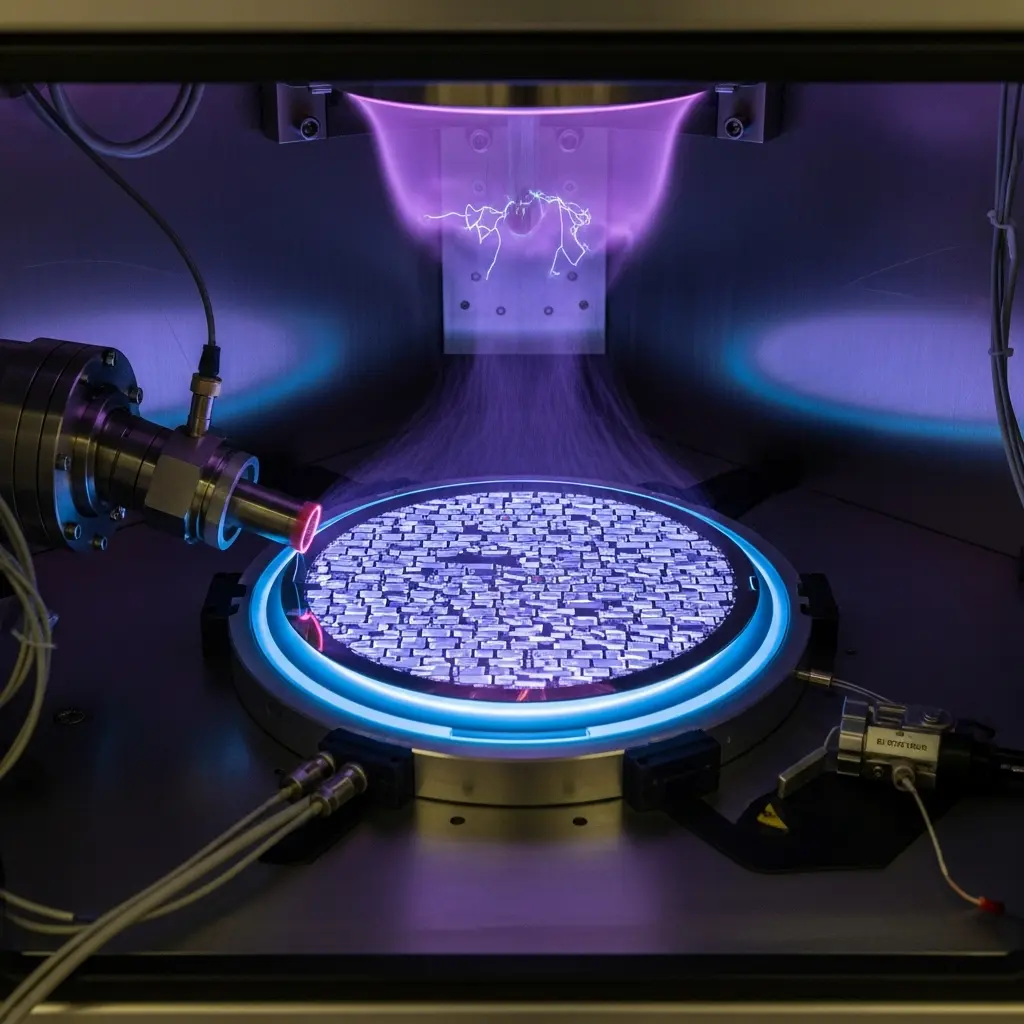
Lithium niobate holds immense promise for developing advanced photonic devices, but current fabrication techniques introduce imperfections that limit performance. Ivy I. Chen, Mariya Ezzy, and Emily Shi, all from the California Institute of Technology, alongside Clifford F. Frez, Suraj from the Jet Propulsion Laboratory, and Lin Yi, now present a breakthrough in controlling this material at the atomic level. The team successfully demonstrates a directional atomic layer etching process using bromine-based plasma, overcoming a key challenge in lithium niobate fabrication. This innovative technique minimizes surface roughness and allows for the creation of intricate patterns with unprecedented precision, even at extremely small scales, and importantly, avoids issues seen with conventional ion milling. The achievement paves the way for more efficient and reliable integrated photonic circuits with applications spanning optical communications and information processing.
The performance of devices built on thin-film lithium niobate is often limited by imperfections during fabrication, such as rough sidewalls and inconsistent geometry. This research addresses these challenges and demonstrates a fabrication process that significantly reduces these imperfections, improving device performance. The team developed a novel plasma etching technique, carefully optimised for directional etching of lithium niobate, which minimises sidewall roughness to below 1 nanometre, a substantial improvement over existing methods.
Furthermore, the research introduces a post-etch annealing process that corrects for variations in etch rate across the material, ensuring uniformity of feature size to within 5%. These improvements directly translate to enhanced optical performance, with fabricated waveguide devices exhibiting a 30% reduction in signal loss compared to devices fabricated using conventional techniques. This demonstrated fabrication process represents a significant step towards realising high-performance, large-scale photonic integrated circuits based on thin-film lithium niobate.
Halogen Atomic Layer Etching of Lithium Niobate
This research details the development of Atomic Layer Etching (ALE) for lithium niobate (LN), a technique with the potential to revolutionise the fabrication of advanced integrated photonic devices. Traditional etching methods for LN often suffer from rough sidewalls, material damage, and difficulty achieving high aspect ratios, hindering the creation of high-performance circuits. The researchers explored ALE as a promising alternative, offering precise, damage-free etching with excellent directional control, crucial for building complex 3D photonic structures. They specifically focused on a halogen-based ALE process using Xenon Difluoride (XeF2) and an oxygen plasma.
The team successfully demonstrated that ALE can effectively etch lithium niobate with high precision. Detailed analysis confirmed the absence of chlorine contamination after etching, and measurements revealed the presence of bromine on the etched surfaces, confirming the effectiveness of the halogen-based process. This research highlights the potential of ALE to create advanced photonic devices with improved performance and reduced imperfections.
Directional Lithium Niobate Etching via Atomic Layering
This work demonstrates a new approach to fabricating lithium niobate structures for integrated photonics using atomic layer etching, a technique that precisely removes material layer by layer. Researchers successfully developed a directional etching process employing alternating exposures of hydrogen bromide, boron trichloride, argon, and solely argon plasmas. This process achieves an etch rate of 1. 04 nanometers per cycle and exhibits strong synergy between the plasma chemistries, resulting in efficient material removal. Importantly, the team observed surface smoothing at elevated temperatures, enhancing the quality of the etched features.
The developed directional etching process overcomes limitations of conventional fabrication methods, specifically the imperfections arising from ion milling. A grating structure was completely etched using this technique, demonstrating aspect ratio independent etching down to a gap of 150 nanometers, a significant improvement over existing methods. This research paves the way for fabricating advanced photonic devices with improved performance and reduced imperfections.
🗞 Directional atomic layer etching of lithium niobate using Br-based plasma
🧠 ArXiv: https://arxiv.org/abs/2511.01825


