Silicon carbide presents a compelling material for next-generation quantum technologies, owing to its ability to host defects with unique quantum properties, but realising its potential requires precise control over these defects within nanoscale devices. Amberly Xie, Aaron Day, and colleagues at Harvard University and IonQ now demonstrate a new fabrication technique to address this challenge, creating suspended silicon carbide membranes suitable for integrating these crucial defects. The team’s approach builds devices directly onto suspended thin films, overcoming the difficulties traditionally associated with processing this robust material, and enabling the creation of structures like photonic and acoustic cavities. This advance promises greater flexibility in device design and fabrication, paving the way for scalable quantum technologies based on silicon carbide.
Integrating these color centers into suspended nanodevices improves defect control and readout, key advances needed to fully harness their potential. However, challenges in developing robust fabrication processes for 4H-SiC thin films, stemming from the material’s chemical and mechanical stability, currently limit its implementation in quantum applications. This work reports a new fabrication approach that first synthesizes suspended thin films from a monolithic platform, and then patterns devices upon them, demonstrating one-dimensional structures.
Fabricating Suspended Silicon Carbide Membranes for Quantum Defects
Researchers addressed challenges in fabricating suspended 4H-Silicon Carbide membranes for integrating defects into quantum devices. A key issue was inconsistent adhesion of a common electron-beam lithography resist, leading to delamination during processing and edge beading. The team systematically tested solutions, including various surface treatments like oxygen plasma, hexamethyldisilazane, and Surpass3000, alongside adjustments to baking temperature and the use of a carrier wafer. Lowering the baking temperature to 115°C and spinning samples on a carrier wafer proved most reliable, ensuring consistent resist adhesion and successful nanofabrication.
This optimization is crucial for creating reliable quantum devices from this material. The researchers also employed computational modeling to design their devices, utilizing Flexcompute Tidy3D for designing one-dimensional photonic crystal cavities and COMSOL Multiphysics for phononic cavities. The availability of the associated code allows other researchers to verify and modify these designs. This computational approach ensures precise device geometry and optimized performance.
Silicon Carbide Nanophotonics via Monolithic Fabrication
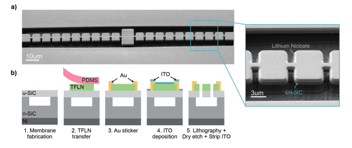
Researchers have developed a new fabrication technique for creating devices from 4H-silicon carbide, a material increasingly important for solid-state technology and quantum applications. The process begins by creating suspended thin films of silicon carbide directly on a monolithic platform, then allows for precise patterning of nanoscale devices onto these films. This approach overcomes limitations in existing fabrication methods, which struggle with the material’s inherent stability and compatibility with diverse materials. The team successfully created photonic crystal cavities, both with and without waveguide interfaces, and integrated lithium niobate onto the silicon carbide platform, demonstrating the versatility of the technique for combining different materials.
Initial tests of these cavities revealed quality factors reaching several thousand, comparable to previously reported results for similar structures in silicon carbide, confirming the effectiveness of the new fabrication process. Importantly, the direct patterning onto suspended films resulted in improved precision and consistency in feature sizes, minimizing fabrication errors. Beyond basic cavity structures, the researchers fabricated tapered waveguide cavities designed to efficiently collect light emitted from defects within the silicon carbide, achieving quality factors exceeding one thousand, paving the way for improved readout efficiency and potential for creating scalable quantum networks. The ability to couple these cavities to optical fibers is a significant step towards long-distance quantum communication and entanglement.
A particularly innovative aspect of the work is the integration of lithium niobate with the silicon carbide platform. This combination allows for the exploration of spin-phonon interactions, offering new avenues for controlling and reading out the state of defects, even those inaccessible through traditional optical methods. The researchers demonstrated a proof-of-concept device integrating thin-film lithium niobate with silicon carbide, showcasing the potential for electrical control and readout of defects via piezoelectric transduction. This opens possibilities for more complex applications, including electro-optic modulation of photons and in-situ tuning of cavities to match the emission wavelength of defects. In summary, this new fabrication technique provides a versatile platform for creating advanced silicon carbide devices with improved precision and material compatibility, promising significant advancements in quantum technologies and beyond.
Monolithic 4H-SiC Photonic Cavities Demonstrated Successfully
This work presents a new fabrication approach for creating devices from 4H-silicon carbide, beginning with the creation of suspended thin films directly from a monolithic platform before device patterning. The researchers successfully demonstrated this technique by fabricating photonic crystal cavities, both with and without waveguide interfaces, and by integrating lithium niobate onto silicon carbide acoustic cavities. These initial devices achieved quality factors of a few thousand, and importantly, represent the first reported demonstration of tapered waveguide cavities within 4H-SiC. The developed method offers increased fabrication flexibility and robustness, particularly at high temperatures, due to the monolithic nature of the suspended films which avoids issues with thermal expansion mismatch seen in composite materials. This platform shows promise for integrating color centers into devices, enabling enhanced spin-state readout and control via piezoelectric transduction and surface acoustic wave generation. While this study serves as a proof-of-concept, the authors acknowledge that further development is needed to fully realize practical spin control and readout capabilities, and suggest future research could explore electro-optic modulation, in-situ cavity tuning, and multiplexing quantum nodes.
👉 More information
🗞 A Suspended 4H-Silicon Carbide Membrane Platform for Defect Integration into Quantum Devices
🧠 ArXiv: https://arxiv.org/abs/2508.10814


