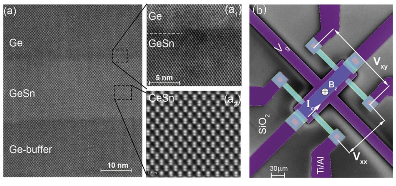
Quantum researchers have turned the spotlight on a humble alloy that could reshape the electronics and quantum‑computing landscapes alike. Germanium‑tin (GeSn) semiconductors, long considered a niche material for specialised optoelectronic devices, have just shown that their internal spin dynamics are far more exotic than previously thought. In a joint effort spanning Germany, Japan, and Canada, scientists have uncovered that holes, the absence of electrons, in GeSn can carry quantum information with remarkable speed and durability, while the material remains fully compatible with the silicon-based chips that power today’s devices.
A New Spin on Semiconductors
The heart of the discovery lies in the behaviour of “heavy holes” confined within a GeSn layer that sits on a germanium substrate. By cooling the structure to a few kelvin and applying a magnetic field, the team measured a large Zeeman splitting, meaning the spin states of the holes separate more sharply than in silicon or pure germanium. This large g-factor, combined with a low in-plane effective mass, enables the holes to respond quickly to electric fields —a key requirement for fast qubit operations. Moreover, the researchers found pronounced anisotropy: the spin response changes depending on the direction of the applied field, offering an additional handle for controlling quantum states.
These properties were revealed through Shubnikov‑de Haas oscillations and Quantum Hall effect measurements, classic techniques for probing electron behaviour in high‑mobility systems. The oscillations persisted at relatively high temperatures, signalling that the holes retain coherence longer than their silicon counterparts. In practical terms, this could translate to qubits that operate reliably at temperatures achievable with compact cryogenic systems, easing the engineering burden on quantum processors.
From Quantum Bits to On‑Chip Lasers
Beyond quantum computing, GeSn’s band structure opens doors to a range of photonic and thermoelectric applications. Its direct-bandgap character, a consequence of the tin addition, makes it an efficient light emitter. In the same study, a transistor fabricated from the material displayed strong electroluminescence, pointing to the feasibility of integrating on‑chip lasers with conventional CMOS circuitry. Such on‑chip light sources are a long‑sought ingredient for silicon photonics, promising faster data links and lower power consumption in data centres.
The alloy’s thermal properties are equally attractive. The lattice mismatch between germanium and tin introduces strain that can be engineered to enhance phonon scattering, improving thermoelectric performance. Early measurements suggest that GeSn layers can convert waste heat into electricity more efficiently than traditional silicon thermoelectrics, offering a path toward self‑powered sensors or cooling solutions for high‑density processors.
Because GeSn can be grown on silicon substrates using standard chemical vapour deposition, the entire stack remains compatible with existing fabrication lines. This compatibility is crucial; it means that the same cleanroom processes that produce billions of transistors each year can also produce quantum‑enabled devices without a costly redesign of the supply chain.
The Road Ahead: Integration and Scaling
The next challenge lies in scaling the material’s advantages from laboratory demonstrations to commercial products. Researchers are already exploring how to shrink the quantum wells to nanometre dimensions while preserving the high mobility and spin coherence. Fine‑tuning the tin concentration will be essential, as it directly controls the bandgap and strain, both of which influence device performance.
Industry players are taking notice. Several semiconductor companies have begun pilot projects to integrate GeSn layers into their next‑generation logic chips, aiming to test the material’s performance under realistic workloads. Meanwhile, quantum‑technology firms are evaluating GeSn as a host for spin‑based qubits, intrigued by the prospect of operating at higher temperatures than the millikelvin environments required for superconducting qubits.
In the broader context, the discovery underscores a growing trend: the search for materials that can bridge the gap between classical electronics and emerging quantum technologies. By delivering both high‑speed spin manipulation and optical functionality, GeSn exemplifies the multifunctional platforms that may define the next decade of computing and communication.
As the semiconductor industry grapples with the limits of silicon, the GeSn breakthrough offers a promising detour. If the material can be mass‑produced with the precision required for high‑performance devices, it could become the backbone of a new generation of electronics that are faster, more energy‑efficient, and capable of harnessing the full power of quantum mechanics.


