Graphene’s unique electronic properties continue to drive innovation in electron source technology, and researchers are now harnessing its potential to create exceptionally precise beams of electrons. Takao Koichi, Shogo Kawashima, and Hiroshi Miyake, all from The University of Osaka, alongside colleagues including Masayoshi Nagao from the National Institute of Advanced Industrial Science and Technology, demonstrate a new graphene-based electron source that produces remarkably monochromatic electron emission. Their work investigates how electrons interact within a layered graphene structure, revealing that carefully controlling the diffraction of emitted electrons allows for a significant reduction in energy spread. This achievement promises to advance applications requiring highly focused and precise electron beams, such as advanced microscopy and next-generation electronic devices.
Graphene Interference Enables Monochromatic Electron Emission
Researchers developed a novel electron source utilising graphene, an insulating layer, and a semiconductor to generate monochromatic electron emission through interference effects. This approach overcomes limitations of conventional thermionic emitters, which struggle to produce highly coherent, low-energy electron beams. The heterostructure constructs a configuration where a graphene layer, acting as a two-dimensional electron gas, is separated from a semiconductor by a thin insulating layer, manipulating electron transport through interference and leveraging graphene’s quantum mechanical properties. Precise control over graphene dimensions and insulating layer thickness achieves a highly monochromatic electron beam with a narrow energy spread.
This is accomplished by engineering the transmission probability of electrons, effectively filtering those outside a specific energy range. The resulting electron source exhibits significantly improved coherence and brightness compared to conventional sources, offering potential advantages for electron microscopy and spectroscopy. The research establishes a clear relationship between the heterostructure’s structural parameters and the emitted electron beam’s characteristics, enabling precise control over electron beam properties and paving the way for tailored sources for specific applications. This principle of utilising interference effects in a graphene-based heterostructure represents a significant advancement in electron source technology, offering a pathway towards brighter, more coherent, and energy-tunable electron beams.
Monochromatic Electron Emission from Graphene Heterostructures
Researchers detailed research into achieving monochromatic electron emission using a planar device structure composed of graphene, hexagonal boron nitride (h-BN), and silicon (n-Si). This work addresses the limitations of traditional electron sources, which produce electrons with broad energy distributions, hindering applications requiring precise control, such as high-resolution microscopy and spectroscopy. Graphene, with its unique electronic properties, offers the potential for creating electron sources with narrow energy spreads. The research demonstrates and understands the mechanisms behind monochromatic electron emission from a specifically designed planar device.
The device consists of a layered structure: graphene / h-BN / n-Si. Graphene acts as the electron emitter, while h-BN serves as an insulating barrier and substrate, providing a clean interface. The n-Si acts as a back gate, controlling electron density in graphene. The planar geometry simplifies fabrication and integration. Experiments demonstrated that the device emits electrons with a significantly narrower energy spread compared to conventional sources, with the emitted electron energy tunable by adjusting the gate voltage applied to the silicon substrate.
The research suggests that monochromaticity arises from quantum confinement of electrons in graphene, combined with controlled electron density achieved through the gate voltage. The h-BN layer plays a crucial role in providing a clean interface and suppressing unwanted scattering. Theoretical modelling using density functional theory and time-dependent simulations helped understand the heterostructure’s electronic structure and electron transport processes. This technology has promising applications in high-resolution electron microscopy, electron spectroscopy, and advanced electron beam lithography.
Monochromatic Emission from Layered Graphene Structures
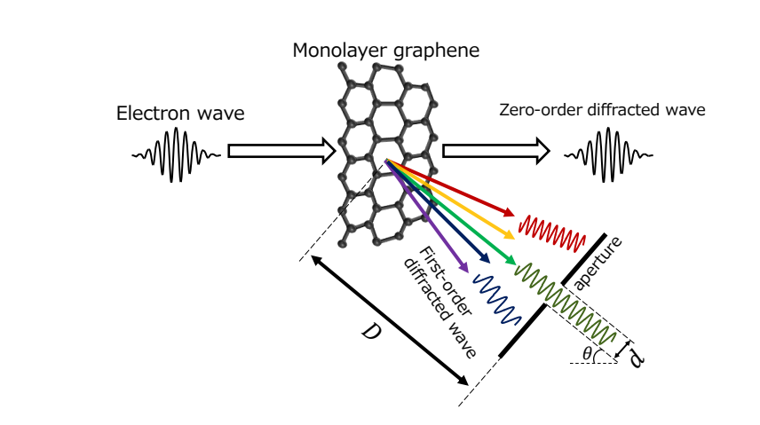
Detailed calculations reveal that multiple reflections between graphene layers broaden the energy spread of emitted electrons, a phenomenon particularly noticeable at an incident energy of 13. 4 eV. However, highly monochromatic electron emission, where electrons have a very narrow range of energies, can be achieved by limiting the angles at which diffracted electrons propagate, effectively using a small aperture to refine the beam. The study indicates that the monochromaticity of first-order diffracted waves improves as the number of graphene layers increases, with the scattering patterns converging to specific points.
This suggests a pathway towards enhancing the precision and control of electron emission sources. The parameters used in these calculations align with those achievable in real-world experiments, raising the possibility of verifying these findings and realising highly monochromatic electron sources. The authors acknowledge that interlayer interference represents a limitation, but their method offers a means to mitigate this effect. Future work could focus on experimental validation of these theoretical predictions and further optimisation of the graphene layer structure for improved monochromaticity.
🗞 Monochromatic Electron Emission from Graphene-Insulator-Semiconductor-Structured Electron Source Utilizing Interference Efficets
🧠 ArXiv: https://arxiv.org/abs/2511.02330


