The electronic properties of layered materials dramatically change when stacked with a slight twist, offering exciting possibilities for band-structure engineering, but real-world devices suffer from imperfections that complicate analysis. Namkyung Lee, Hangyeol Park, Seungwon Jung, and colleagues at Seoul National University have now developed a technique to map the local electronic structure and twist angle in these twisted van der Waals heterostructures with unprecedented precision. The team employs Kelvin probe force microscopy to measure the local thermodynamic density of states, revealing variations in twist angle and their correlation with strain features caused by trapped bubbles. Crucially, they demonstrate the ability to pinpoint exactly which layer hosts these bubbles, offering a powerful tool for understanding and controlling strain in nanoscale moiré systems and paving the way for advanced device designs.
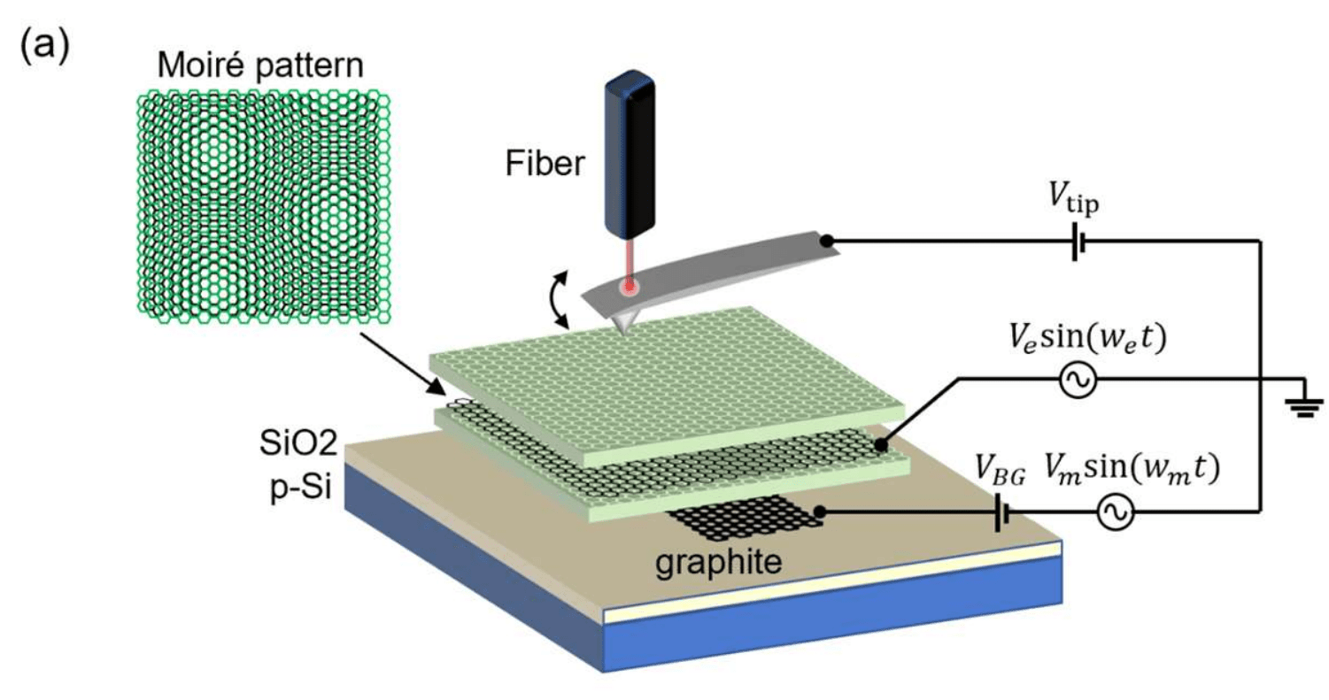
Twisted van der Waals stacks fundamentally reshape electronic properties, enabling band-structure engineering that has driven rapidly growing interest in this field. However, structural disorder present in real devices often leads to twist-angle inhomogeneity and obscures angle-dependent electronic effects when measured with bulk-averaged techniques. Probes that can access the local thermodynamic response of electronic systems with high sensitivity are therefore highly valuable. This work adopts Kelvin probe force microscopy (KPFM) to locally investigate graphene-hBN superlattices, and additionally modulates the chemical potential.
Disorder’s Impact on Twisted Bilayer Graphene
This research focuses on twisted bilayer graphene and other two-dimensional material heterostructures where the stacking angle dramatically affects electronic properties, including the creation of exotic states like superconductivity. A major challenge in realizing these properties is disorder, encompassing imperfections in stacking, lattice relaxation, and variations in the twist angle, which can disrupt delicate electronic states. Consequently, there is a critical need to characterize this disorder at high resolution to understand and control the properties of these materials. The team employed KPFM, a scanning probe microscopy method that measures the contact potential difference between the tip and the sample surface, allowing them to map the local chemical potential.
By creating high-resolution maps, the researchers correlated variations with the underlying Moiré pattern. The KPFM data reveals variations in the local chemical potential that directly correlate with variations in the twist angle, effectively mapping the twist angle distribution across the sample. They identified domains with different twist angles and observed evidence of lattice relaxation, indicating that the atoms are not perfectly arranged as predicted by simple theory. By characterizing the twist angle distribution, researchers can potentially control the electronic properties of these materials, contributing to the broader field of two-dimensional materials research and potentially leading to the development of new electronic devices. This research provides a crucial tool for understanding the role of disorder and relaxation in moiré materials.
Local Twist Angle Maps Electronic Properties
Researchers have achieved a breakthrough in characterizing local electronic properties within twisted van der Waals heterostructures, employing Kelvin probe force microscopy (KPFM) to map variations in chemical potential with unprecedented sensitivity. The study demonstrates the ability to locally measure inverse compressibility, enabling determination of the local twist angle and revealing strong correlations between twist-angle deviations and bubble-induced strain features. Experiments show that variations in twist angle directly impact the electronic landscape of these materials, providing insights into the origins of emergent phenomena. The team successfully identified interfaces within the heterostructure that host trapped bubbles by simultaneously tracking changes in both contact potential difference and net charge, a capability that provides a practical tool for strain-based studies and future nanoscale device designs.
Measurements confirm that the KPFM technique can resolve local variations in chemical potential with high signal-to-noise ratio, allowing for precise mapping of the electronic landscape. Data shows that the measured twist angles correlate directly with the presence of strain features induced by bubbles, providing a clear link between structural defects and electronic properties. This work delivers a new method for characterizing the complex interplay between twist angle, strain, and electronic behavior in moiré materials, achieving a spatial resolution sufficient to probe the local thermodynamic density of states. This breakthrough provides a powerful tool for understanding and engineering the unique electronic properties of twisted van der Waals heterostructures, paving the way for advanced nanoscale devices.
Mapping Twist Angles and Bubble Locations
This research demonstrates a new method for characterizing local electronic properties and structural features within twisted van der Waals heterostructures, specifically graphene layered with hexagonal boron nitride. By employing Kelvin probe force microscopy, scientists successfully measured the local thermodynamic density of states, revealing a direct correlation between variations in electronic properties and the presence of twist-angle inhomogeneity. The technique allows reconstruction of the device’s twist-angle landscape with high sensitivity, identifying regions where the layers are misaligned. Importantly, the team extended this capability to pinpoint the vertical location of trapped bubbles within the heterostructure, determining whether they reside at the interface between graphene and hexagonal boron nitride, or between the hexagonal boron nitride and the substrate.
This identification is achieved by simultaneously tracking changes in contact potential and net charge, providing valuable insight into the device’s structural characteristics. This advancement offers a practical route for strain-resolved studies and future nanoscale engineering of moiré systems, potentially leading to improved device designs and performance. By characterizing local electronic properties and structural features, this research provides a valuable tool for advancing the field of two-dimensional materials and developing new electronic devices.
👉 More information
🗞 Local thermodynamic DOS measurement and twist-angle mapping in graphene-hBN superlattices
🧠 ArXiv: https://arxiv.org/abs/2511.01246


