Controlling the initial growth of gallium nitride (GaN) is crucial for advanced semiconductor manufacturing, and researchers are now demonstrating unprecedented control using graphene masks perforated with nanoscale holes, allowing GaN to grow through them. Su Young An and Chinkyo Kim, from Kyung Hee University, lead a team that precisely tunes the density of these holes using oxygen plasma, and then investigates how this impacts the very first stages of GaN crystal formation. The results reveal a direct relationship between the hole density and both how quickly GaN begins to grow and how many individual crystals form, offering a way to engineer the nucleation process. By combining experiments with computer simulations, the team establishes a single, controllable parameter for optimising GaN growth on these masks, paving the way for more efficient and precise manufacturing of high-performance semiconductor devices using techniques like epitaxial lateral overgrowth and thru-hole epitaxy.
The density of perforations, determined by oxygen-plasma exposure, directly impacts the early stages of nucleation. The number of nucleation sites scales with perforation density, while the time required for nucleation decreases predictably as density increases. Time-resolved measurements reveal systematic trends related to perforation density, and a computational model, based on kinetic Monte Carlo (kMC) simulations, accurately reproduces these trends by simulating GaN atom arrival, surface diffusion, and domain formation, using a constant nucleation rate. Fitting the kMC simulation data yields information about the delay before nucleation begins.
Plasma Exposure Modifies GaN Growth Morphology
This document provides comprehensive supplementary information detailing the research on controlling GaN nucleation, presenting a strong foundation of data supporting the main publication’s claims with clear organization and detailed analysis. It includes high-quality SEM images and additional plots illustrating the effects of plasma exposure time on GaN growth. Overall Strengths: * Clear Organization: The document is well-structured, with clear headings and figure captions. * Detailed Supplementary Data: It provides crucial data, such as SEM images and plots, supporting the main publication’s claims.
- Strong Visuals: The SEM images are high quality and clearly illustrate the effect of plasma exposure time on GaN growth, and the plots are well-labeled and easy to interpret. * Quantitative Support: The additional plots provide quantitative backing for the qualitative observations. The comparison between experimental data and the kMC simulation is particularly strong. * Completeness: It feels like a complete package, with no obvious gaps in the information presented. * Concise and Focused: The supplementary information stays focused on supporting the main publication’s claims, avoiding unrelated topics.
Summary of Content: This supplementary information provides additional data and analysis supporting the findings on controlling GaN nucleation using O2-plasma-perforated graphene masks. Specifically, it includes: * SEM Images: High-resolution images showing the morphology of GaN domains grown with varying O2 plasma exposure times and growth durations, visually demonstrating the effect of plasma treatment on the density and distribution of GaN domains. * Additional Plots: * Domain Count vs. Growth Duration: Plots showing the number of isolated GaN domains per circular opening as a function of growth duration for different O2 plasma exposure times.
- Areal Fraction vs. Growth Duration: Plots showing the areal fraction of GaN coverage as a function of growth duration for different O2 plasma exposure times. * Comparison with kMC Simulation: Plots comparing the experimental data for domain count and areal fraction with the results of a kinetic Monte Carlo (kMC) simulation, demonstrating the ability of the model to reproduce the experimental observations. Overall Assessment: This is an excellent example of supplementary information, well-organized, comprehensive, and providing strong support for the main publication’s claims. The inclusion of both visual data (SEM images) and quantitative data (plots) is particularly effective, and the comparison with the kMC simulation adds a layer of theoretical validation.
Graphene Masks Control Gallium Nitride Growth
This research demonstrates that multilayer graphene grown on sapphire can function as a nanoscale mask for growing gallium nitride (GaN) through tiny holes, a process relevant to creating advanced electronic devices. The team successfully controlled the density of these holes by adjusting oxygen plasma exposure during graphene preparation, and quantified the relationship between hole density and the initiation of GaN growth. A higher density of holes correlates with a faster start to GaN growth, and the delay before growth begins decreases predictably with increased hole density.
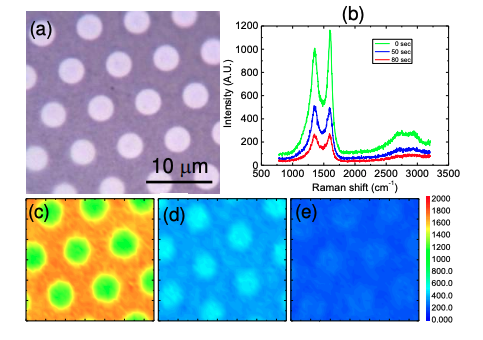
To understand this process, the researchers developed a computational model that simulates the arrival and attachment of GaN atoms on the graphene mask. This model accurately reproduces the experimental observations, confirming that the plasma treatment establishes a clear threshold for creating the through-holes necessary for GaN growth. Raman spectroscopy further confirmed the graphene layer remains intact beneath the grown GaN. These findings establish a scalable method for controlling GaN nucleation, offering a pathway to engineer materials for applications such as LEDs and high-power electronics.
🗞 Controlling GaN nucleation via O -plasma-perforated graphene masks on c-plane sapphire
🧠 ArXiv: https://arxiv.org/abs/2509.08275


