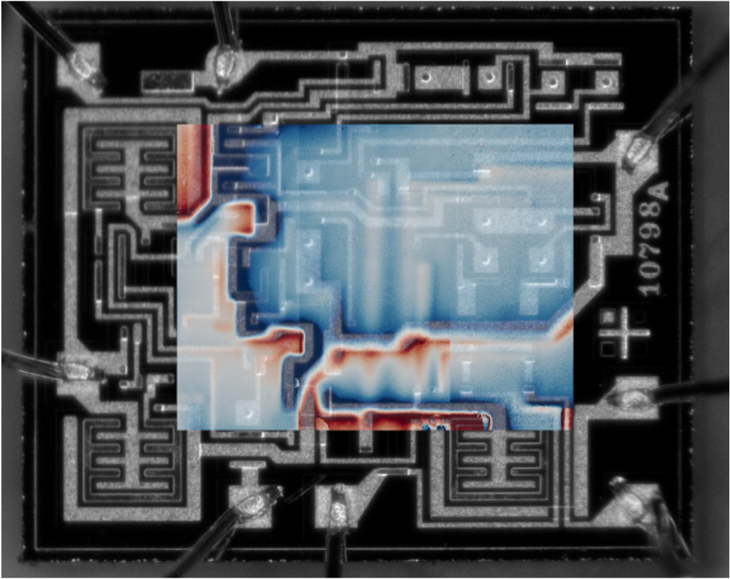
Forget peeling back layers or relying on guesswork – a new platform is promising to see inside the very heart of semiconductors and batteries. Emerging from stealth mode with significant funding and early revenue, EuQlid is bringing quantum precision to industrial-scale imaging, tackling a critical bottleneck in both the chip and energy storage industries. Their breakthrough technology maps sub-surface electrical currents with unprecedented detail and speed, offering a non-destructive way to optimize manufacturing, improve yields, and unlock the potential of increasingly complex 3D designs – a necessity fueled by the booming demand for AI and advanced computing.
EuQlid’s Quantum Imaging Platform: Qu-MRI
EuQlid has emerged from stealth mode with a novel 3D imaging platform, Qu-MRI™, poised to address critical metrology gaps in the semiconductor and battery industries. This quantum-based technology utilizes quantum magnetometry, advanced signal processing, and machine learning to non-destructively map sub-surface electrical currents with nano-amp sensitivity. Unlike current inspection methods, Qu-MRI™ requires no physical contact or destructive cross-sectioning, offering high-throughput analysis of buried current flow. Applications range from spatial analysis of power flows within functioning CPUs and GPUs to detecting interconnect errors in high-bandwidth memory manufacturing. Backed by $3 million in funding and early customer revenue exceeding $1.5 million, EuQlid aims to deliver “quantum precision” for both research and development labs and high-volume manufacturing environments, capitalizing on a $10 billion-plus global market for advanced metrology tools.
Addressing Critical Industry Gaps
EuQlid is poised to disrupt semiconductor and battery manufacturing by directly addressing a critical gap in current metrology tools. The company’s Qu-MRITM platform utilizes quantum magnetometry to deliver non-invasive, high-throughput 3D imaging of sub-surface electrical currents—a capability unavailable with existing technologies. This breakthrough allows for the visualization of buried connectivity defects and spatial analysis of power flows within functioning devices like CPUs and GPUs, offering crucial insights for both research & development and high-volume manufacturing. With a market exceeding $10 billion annually and rapidly expanding due to the demand for complex 3D architectures driven by AI, EuQlid’s technology promises to optimize manufacturing workflows, improve yields, and accelerate innovation in these rapidly evolving industries. Backed by $3 million in funding and early customer revenue exceeding $1.5 million, the company is transitioning quantum science into fab-ready tools.
Scaling Quantum Precision for Manufacturing
EuQlid is poised to address a critical need in advanced manufacturing with its Qu-MRI platform, a quantum-based imaging solution designed for non-destructive, high-throughput inspection of semiconductors and batteries. The company recently emerged from stealth with $3 million in funding and early revenue, aiming to fill a gap in current metrology tools – namely, the ability to visualize sub-surface electrical currents with nanoscale precision. This capability is increasingly vital as the semiconductor industry adopts complex 3D architectures to meet the demands of AI and high-performance computing. Unlike traditional methods requiring physical cross-sectioning, Qu-MRI uses quantum magnetometry and machine learning to map buried current flow, offering insights into defects like interconnect stacking errors and spatial analysis of power flows within functioning chips – all without damaging the device. With a market exceeding $10 billion annually, EuQlid’s technology seeks to bring “quantum precision” to both R&D and high-volume manufacturing environments.
Source: https://euqlid.io/


