The subtle interplay of electron behaviour within layered materials drives advances in modern electronics, and recent research focuses on understanding these interactions in twisted bilayer graphene. Alexey A. Sokolik, from the Institute for Spectroscopy and National Research University Higher School of Economics, alongside Azat F. Aminov from the same institution, and Evgenii E. Vdovin and Yurii N. Khanin from the Institute of Microelectronics Technology and High Purity Materials, demonstrate a novel method for probing the features of electron dispersion by measuring tunneling between slightly twisted bilayer graphene sheets. This work reveals how the heavier effective mass of holes enhances tunneling conductance at higher doping levels, and crucially, identifies asymmetric tunneling resonances arising from the opening of an energy gap in a vertical electric field. By combining experimental measurements with a detailed theoretical model, the team demonstrates a strong sensitivity of tunneling current to minor changes in gate voltages, paving the way for highly sensitive electronic devices and a deeper understanding of electron behaviour in two-dimensional materials.
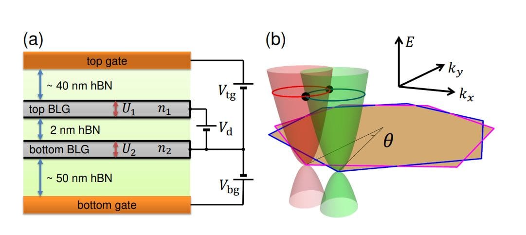
Tunneling conductance between two bilayer graphene (BLG) sheets separated by a 2nm-thick insulating barrier was measured in devices with slightly different twist angles. This research investigates how the relative orientation of graphene layers impacts electron tunneling, a quantum mechanical phenomenon crucial for understanding the electronic properties of these materials. The team fabricated devices with precisely controlled interlayer spacing and twist angle, then meticulously characterized their electrical transport properties at low temperatures. Bernal bilayer graphene and hBN flakes were mechanically exfoliated onto a silicon dioxide substrate, then precisely positioned using a polymer stamp to create the desired heterostructure. Crucially, adjacent graphene flakes from the same exfoliation were used to ensure a near-zero twist angle, minimizing interference in the tunneling measurements. Device 1 incorporated a silicon substrate with a 300nm thick silicon dioxide dielectric, while Device 2 utilized a graphite flake, resulting in twist angles of approximately 0.
7° and 0. 1° respectively. Electrical contacts were defined using electron beam lithography, followed by deposition and lift-off of chromium and gold. The active areas of the devices, representing the overlapping graphene flakes, were approximately 1.
4 μm² for Device 1 and 18 μm² for Device 2, influencing the magnitude of the measured tunneling current. A detailed electrostatic model describes the behaviour of electrons within the heterostructure, utilizing Gauss’s law to relate electron densities in the top and bottom bilayer graphene sheets to the electric fields within the insulating layers. By connecting these laws, researchers established relationships with internal fields, enabling the calculation of electron densities and induced gaps. The model accounts for external voltages applied to the top and bottom gates, as well as the potential differences between the graphene layers, providing a comprehensive framework for understanding the observed tunneling phenomena. Solving a system of equations, incorporating parameters like dielectric constants and inter-sublayer capacitance, determined key variables such as chemical potentials and induced gaps, ultimately enabling the calculation of tunneling conductance.
Twist Angle Impacts Conductance Calculations
Supplementary information details the methods and calculations used in a study of tunneling conductance in bilayer graphene (BLG) devices with varying twist angles, aiming to explain the computational methods, validate the modeling approach, and allow for reproducibility of the findings. The document specifies parameters used to describe the electronic band structure of BLG, assumes a dielectric constant for hexagonal boron nitride (hBN), and defines the temperature and energy width used in the calculations. The detailed methods section explains how the tunneling conductance maps were normalized using electric fields instead of gate voltages, and presents a series of calculated tunneling conductance maps for twist angles ranging from 0. 1° to 0.
6°. Calculated tunneling conductance along specific cross-sections of the maps is also presented. Supporting figures compare experimental and theoretical tunneling conductance maps for Devices 1 and 2 in terms of electric fields, and present a series of calculated tunneling conductance maps for different twist angles. The calculations demonstrate that the twist angle significantly affects the tunneling conductance, widening allowed tunneling regions and creating forbidden regions as the angle increases. An asymmetric tunneling resonance develops at twist angles greater than or equal to 0. 3°. The heavier nature of holes within the graphene structure enhances tunneling at higher hole doping levels, due to an increased density of available states. Furthermore, the application of a vertical electric field induces polarization of electron wave functions, leading to asymmetric tunneling resonances and a strong sensitivity of the tunneling current to minor changes in gate voltage. These observations are supported by a theoretical model that accurately accounts for the electrostatic properties of the device, quantum capacitance effects, and the self-consistent opening of energy gaps within the graphene layers.
Researchers mapped regions where tunneling is permitted or forbidden based on energy and momentum conservation laws, and the magnitude of the tunneling conductance clearly demonstrated the observed electron-hole asymmetry. While acknowledging that the current study focuses on small twist angles, the authors suggest that quantum twisting microscopy holds significant promise for investigating the electronic properties of two-dimensional materials. Future work may explore the potential of manipulating tunneling conductance through twist angle, electrical doping, and applied electric fields to create novel nanoscale electronic devices.
👉 More information
🗞 Probing the features of electron dispersion by tunneling between slightly twisted bilayer graphene sheets
🧠 ArXiv: https://arxiv.org/abs/2511.09550


