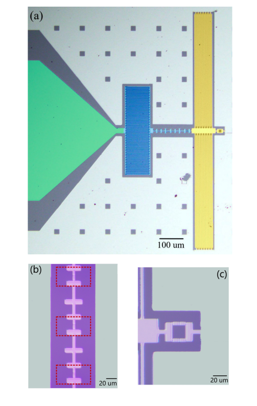
The quest for highly sensitive detectors is crucial for advances in fields ranging from astronomy to quantum computing, and researchers are continually seeking ways to amplify the extremely weak signals these applications require. Lipi Patel, Samarth Hawaldar, and colleagues at the Indian Institute of Science, along with Aditya Panikkar and Athreya Shankar from the Indian Institute of Technology Madras, now demonstrate a significant step forward in this area with a new type of amplifier built using a simplified fabrication process. Their work centres on a Josephson parametric amplifier, enhanced through careful control of its electrical environment , a technique known as impedance engineering , and crucially, realised with a single lithography step. This streamlined approach, combined with the amplifier’s impressive performance , achieving 18 decibels of gain across a 400 megahertz bandwidth , paves the way for more accessible and scalable production of broadband amplifiers, and offers new insights into how these devices operate at their limits.
Simplified Fabrication Boosts Quantum Amplifier Performance
Researchers have demonstrated a significant advancement in the design and fabrication of Josephson Parametric Amplifiers (JPAs), crucial components in superconducting quantum circuits for sensitive detection of quantum information. This work addresses the complexity of traditional JPA fabrication by presenting a device with a simplified, single-step lithography process, paving the way for more accessible and reliable quantum technologies.
Current JPAs often require multiple lithography steps, but this innovation streamlines fabrication and minimizes potential errors, leading to more reliable devices with high gain over a wide bandwidth, comparable to state-of-the-art designs. The core of this advancement is impedance engineering, a technique that optimizes how the amplifier interacts with external circuits, broadening the amplifier’s bandwidth without sacrificing gain, particularly important for applications like multiplexed qubit readout.
Researchers also developed a refined theoretical model to accurately predict the amplifier’s performance, validating the experimental results and providing a foundation for designing even more advanced JPAs. By simplifying fabrication and improving performance, this research represents a significant step towards building more practical and scalable quantum technologies.
Fabrication of Superconducting Josephson Parametric Amplifier
The device fabrication involves creating an impedance-engineered Josephson Parametric Amplifier (JPA) using advanced lithographic techniques, comprising a Josephson junction array forming an impedance transformer coupled to a SQUID-based amplifier. The entire device is constructed from coplanar elements on an intrinsic silicon substrate, beginning with substrate cleaning using a piranha solution and dilute hydrofluoric acid.
A resist bilayer is then spin-coated onto the substrate, followed by patterning using electron-beam lithography. Josephson junctions are formed using standard deposition and etching techniques, and the device is packaged for testing and characterization.
The resulting amplifier exhibits excellent performance characteristics, including high gain and low noise, making it suitable for quantum computing and sensing.
Broadband Amplifier Rivals State-of-the-Art Performance
Researchers have fabricated and characterized a broadband impedance-engineered Josephson Parametric Amplifier (IEJPA), achieving a gain of 18 dB over a 400 MHz bandwidth with near quantum-limited noise performance and a saturation power of −114 dBm. These results are comparable to state-of-the-art values, demonstrating the effectiveness of the simplified fabrication process and making the amplifier suitable for a wide range of applications.
Experimental results align with theoretical models, validating the design and fabrication process. Further improvements could involve increasing saturation power and reducing transformer nonlinearity. Similar devices can be designed using three-wave mixing, allowing for easier filtering of the pump tone, and the compact footprint enables on-chip integration into a qubit architecture, mitigating insertion loss.
Acknowledgements: This work was supported by the Space Technology Cell at IISc and ISRO, the Ministry of Electronics and Information Technology of the Govt. of India, and the Office of Principle Scientific Advisor, Govt. of India. Researchers acknowledge the support of the Kishore Vaigyanik Protsahan Yojana (KVPY) and a New Faculty Initiation Grant (NFIG) from IIT Madras.
Data Availability: The data that support the findings of this study are available from the corresponding author upon reasonable request.
🗞 Impedance-Engineered Josephson Parametric Amplifier with Single-Step Lithography
🧠 DOI: https://doi.org/10.48550/arXiv.2507.09298


