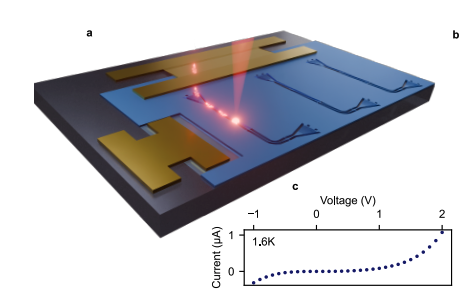
The demand for scalable quantum technologies drives research into integrating high-performance light sources with established silicon photonics, and a team led by Hanna at the University of Cambridge now presents a significant step forward in this area. Researchers successfully demonstrate electrical control of quantum dots embedded within gallium arsenide waveguides bonded onto a silicon substrate, effectively creating a platform for generating coherent single photons. This innovative approach utilises a bonding process to build a gallium arsenide-on-insulator structure incorporating a junction that suppresses disruptive charge noise and allows precise tuning of the quantum dots’ light-emitting properties. The resulting devices exhibit narrow linewidths and high single-photon purity comparable to unprocessed materials, establishing a practical pathway to integrate high-coherence light sources with silicon photonics and paving the way for scalable photonic integrated circuits.
This work combines the efficient single-photon emission of GaAs quantum dots with the low-loss waveguides of silicon photonics, creating a promising platform for scalable quantum technologies. Detailed characterization reveals high single-photon purity and indistinguishability, demonstrating the potential for creating complex quantum circuits. The researchers observed distinct emission lines, potentially originating from different charge states or neighbouring emitters.
Strategies to mitigate broadening of these emissions include reducing excitation power and embedding the emitters within an optical cavity. High single-photon purity was confirmed using a Mach-Zehnder interferometer, with measurements showing a value of 3. 7 ± 1. 9%, and Hong-Ou-Mandel interference measurements demonstrated high photon indistinguishability, even at high excitation powers. The fabrication process relies on carefully designed adiabatic tapers to couple light from the GaAs waveguide to the SiN waveguide, achieving approximately 65% efficiency with fabrication accuracy better than 10 nanometres.
This level of detail is crucial for reproducibility and further optimization, representing a significant step towards building scalable quantum photonic circuits with low loss and high efficiency. The high-performance single-photon sources developed in this work could be used in various quantum applications, including quantum communication, quantum computing, and quantum sensing. The successful demonstration of hybrid integration between GaAs and SiN opens up possibilities for integrating other materials and devices onto the same platform.
GaAs Quantum Dots Integrated with Silicon Photonics
Researchers have successfully integrated high-quality, solid-state light sources with silicon photonics, a crucial step towards scalable quantum technologies. The team demonstrated a method for transferring gallium arsenide (GaAs) membranes, containing embedded quantum dots, onto a silica platform and then coupling them to silicon nitride waveguides. This approach efficiently combines the desirable properties of solid-state emitters with the mature manufacturing processes of silicon-based circuits, maintaining the high coherence of the quantum dots essential for applications like quantum communication and computation. A significant aspect of this work is the preservation of emitter performance during the transfer process, with narrow optical linewidths, below 2 micro-electronvolts, and high single-photon purity comparable to unprocessed GaAs material.
The team also incorporated a p-i-n junction within the GaAs membrane, enabling electrical control to suppress noise and fine-tune the emission wavelength. The fabrication process relies on die-to-die bonding, a relatively inexpensive and scalable technique, with electrical characteristics of the p-i-n diode remaining functional after transfer, exhibiting low leakage currents and minimal power consumption, making it compatible with existing CMOS electronics. This compatibility is vital for creating complex, integrated quantum circuits. By combining the high performance of GaAs quantum dots with the manufacturing advantages of silicon photonics, researchers are closer to realizing practical quantum communication networks and advanced quantum technologies, with the ability to electrically control and tune the emitters further enhancing the potential for versatile and adaptable quantum devices.
Silicon Photonics Integrates Electrically Controlled Quantum Dots
This research successfully integrates electrically controlled quantum dots into a silicon photonic platform, representing a significant step towards scalable quantum photonic circuits. The team demonstrated a method for bonding gallium arsenide, containing the quantum dots, onto a silicon substrate and then coupling it to silicon nitride waveguides, maintaining high coherence and narrow optical linewidths comparable to unprocessed gallium arsenide, while also enabling electrical control of the emitted photons. This achievement establishes a practical route for combining high-performance single-photon sources with mature silicon photonics technology. The demonstrated fabrication process, involving die-to-die bonding, offers a potentially scalable and cost-effective approach, particularly when combined with epitaxial lift-off techniques for substrate reuse. While the current work achieves a coupling efficiency of approximately 65%, the authors acknowledge that further improvements are possible through optimization of taper geometries and alignment accuracy, with future research focusing on enhancing photon extraction efficiency and exploring other heterogeneous integration techniques.
🗞 Electrical control of quantum dots in GaAs-on-insulator waveguides for coherent single-photon generation
🧠 ArXiv: https://arxiv.org/abs/2508.04584


