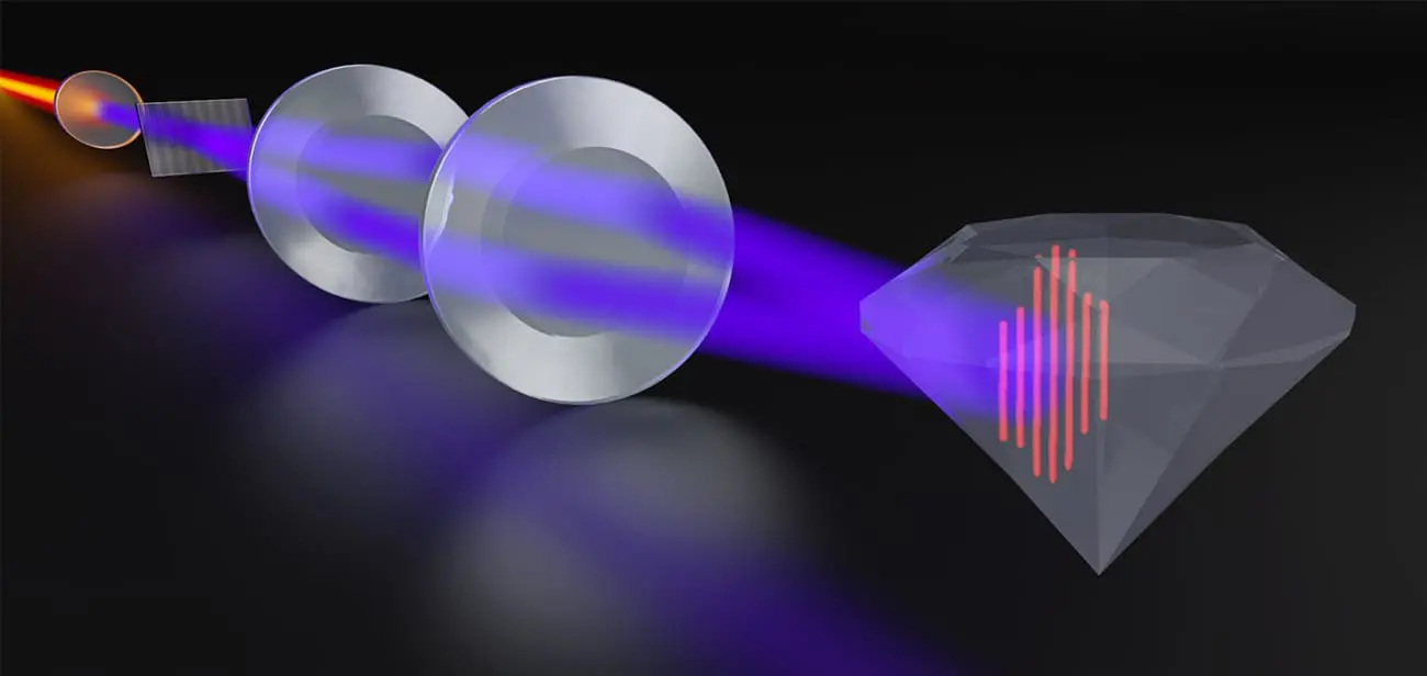
The pursuit of next-generation electronics has led researchers to ultrawide-bandgap semiconductors, such as diamond, which boast a larger energy gap between their valence and conduction bands, enabling them to handle higher voltages, operate at higher frequencies, and provide greater efficiency compared to traditional materials like silicon.
However, the unique properties of these materials have made it challenging to probe and understand how charge and heat move on nanometer-to-micron scales, hindering their widespread adoption in high-performance power electronics, efficient communication systems, and quantum technologies.
To overcome this hurdle, a team of researchers at JILA has developed a novel microscope that utilizes deep-ultraviolet laser light to create a nanoscale interference pattern on a material’s surface, allowing for the examination of electronic, thermal, and mechanical properties with unprecedented spatial resolutions as fine as 287 nanometers, paving the way for a deeper understanding of ultrawide-bandgap materials and their potential applications in future devices.
Introduction to Ultrawide-Bandgap Semiconductors
Ultrawide-bandgap semiconductors, such as diamond, have been gaining attention in recent years due to their exceptional electronic and thermal properties. These materials have the potential to revolutionize various fields, including power electronics, communication systems, and quantum technologies. However, studying these materials at the nanoscale has proven to be a significant challenge. Traditional techniques using visible light are limited by their spatial resolution and inability to interact with electrons in these materials.
Overcoming Limitations with Deep Ultraviolet Light
To overcome these limitations, researchers have turned to deep ultraviolet (DUV) light, which has higher energy photons that can interact with electrons in ultrawide-bandgap semiconductors. By using DUV light, researchers can generate nanoscale heat patterns on a material’s surface without altering the material itself. This approach enables the study of these materials in their pristine state, providing valuable insights into their properties and behavior.
Development of a Compact DUV Microscope
A team of researchers has developed a compact microscope that uses DUV light to generate nanoscale heat patterns on a material’s surface. The microscope uses a laser emitting pulses at an 800-nanometer wavelength, which is then converted into shorter wavelengths through nonlinear crystals. This process ultimately produces a powerful DUV light source at around 200 nanometers wavelength. The researchers split the DUV light into two identical beams using a diffraction grating, which are directed onto the material’s surface at slightly different angles, forming a precise sinusoidal pattern of alternating high and low energy.
Testing the New DUV Microscope
The team tested their new DUV microscope by validating its accuracy and exploring its capabilities. They used thin gold films as a benchmark material due to their well-understood properties. The researchers generated nanoscale heat patterns, launching acoustic waves at the film’s surface, and analyzed the frequency and behavior of these waves to extract material properties such as density and elasticity. The experimental data matched closely with computer models simulating how the gold film would behave under similar conditions.
Studying Diamond with the DUV Microscope
The team then used their new DUV microscope to study diamond, a material prized for its exceptional electronic and thermal properties. Previous techniques for studying diamond often required physical alterations, which inadvertently changed its properties. The DUV system eliminated this need, enabling the team to study diamond in its pristine state. Using their new setup, the researchers observed how charge carriers—electrons and holes—diffused across the diamond after being excited by the DUV light. This process revealed new insights into the nanoscale transport dynamics of diamonds, particularly at nanometer scales.
Implications for Nanoscale Heat Transport
The team’s findings shed light on broader questions of nanoscale heat transport. At such small scales, heat doesn’t always behave as predicted by traditional physical models, which assume a smooth, continuous flow. Instead, nanoscale transport can involve ballistic and hydrodynamic effects, where energy carriers like phonons can travel in a straight line without scattering or can spread like water flowing through channels. As researchers continue to refine these techniques and explore new materials, this advancement could play a crucial role in the development of high-performance power electronics, efficient communication systems, and quantum technologies.
External Link: Click Here For More


