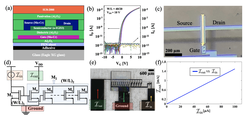
The Diamond Microscope successfully maps current flow within a 16-transistor amorphous-indium-gallium-zinc oxide thin-film circuit at wafer level. Magnetic field imaging via the Diamond Microscope accurately reproduces electrical measurements and visualises current paths inaccessible by conventional probing, offering a non-invasive diagnostic tool for flexible electronics fabrication.
Visualising electrical current flow within integrated circuits presents a significant challenge for fabrication and quality control, particularly as devices shrink and complexity increases. Traditional electrical probing methods offer limited access to internal circuit pathways and can disrupt sensitive components. Researchers are now employing a novel technique, utilising the sensitivity of nitrogen-vacancy (NV) centres in diamond to map current distributions non-invasively. A collaborative team comprising Mayana Yousuf Ali Khan, Pralekh Dubey, and Phani Kumar Peddibothla from the Indian Institute of Science Education and Research, Bhopal, alongside Lakshmi Madhuri P, Ashutosh Kumar Tripathi, and Pydi Ganga Bahubalindruni from the Indian Institute of Technology, Kanpur, detail their work in a recent publication titled ‘Sensing Electric Currents in an a-IGZO TFT-Based Circuit Using a Quantum Diamond Microscope’. Their study demonstrates the successful application of a quantum diamond microscope (QDM) to characterise current flow within a 16-transistor current mirror circuit fabricated using amorphous-indium-gallium-zinc oxide (a-IGZO) thin-film transistors, a material favoured for its potential in flexible electronics.
Quantum diamond microscopy accurately visualises current flow in thin-film transistors, establishing a powerful new technique for semiconductor characterisation and quality control. Researchers successfully applied the Quantum Diamond Microscope (QDM) to characterise current flow within a functional, wafer-level current mirror circuit fabricated using amorphous-indium-gallium-zinc oxide (a-IGZO) thin-film transistors. The QDM accurately maps current densities through non-invasive magnetic field imaging, providing spatially resolved data that corroborates conventional electrical probing techniques and establishes QDM as a reliable method for assessing semiconductor device functionality. This innovative approach offers a significant advantage over traditional methods, enabling researchers to visualise current pathways inaccessible to standard electrical measurements and providing a more comprehensive understanding of circuit behaviour.
QDM operates by detecting the magnetic fields generated by direct currents, producing two-dimensional images that reveal current distribution within the circuit and allowing for detailed analysis of electrical activity. The team extracts accurate current density maps from these magnetic field images, confirming the technique’s quantitative accuracy. Crucially, measurements obtained via QDM correlate strongly with those derived from conventional electrical probing techniques, establishing QDM as a valuable tool for semiconductor characterisation.
Previous work established the foundations of this technology, including studies by Reuss et al. (2005) and Nomura et al. (2004) which explored the potential of diamond-based sensing. Foundational work by Gruber et al. (1997) and Doherty et al. (2013) established the principles of nitrogen-vacancy (NV) centre magnetometry, a key component of QDM, and demonstrated the potential of NV centres for sensitive magnetic field detection. Nitrogen-vacancy centres are point defects in the diamond lattice, created by replacing a carbon atom with a nitrogen atom and leaving a vacancy next to it. These centres exhibit quantum mechanical properties that make them exceptionally sensitive to magnetic fields. These earlier studies provided the theoretical and experimental basis for the development of QDM, enabling researchers to harness the unique properties of NV centres for advanced imaging and analysis. Further research by Roth et al. (1989), Tetienne et al. (2019), Broadway et al. (2020) and Abrahams et al. (2021) contributed to the understanding of the underlying physics and practical applications of this technology, refining the technique and expanding its capabilities.
This technique’s sensitivity to current flow allows for detailed analysis of transistor behaviour and identification of process-induced variations. This non-destructive means of optimising fabrication and performance proves particularly valuable for characterising emerging semiconductor technologies, specifically oxide-based thin-film transistors like those utilising a-IGZO. These materials are gaining prominence in flexible electronics due to their favourable properties, and QDM offers a non-destructive means of optimising their fabrication and performance. By providing detailed insights into current distribution, QDM assists fabrication engineers in optimising manufacturing processes, improving yield, and enhancing the overall reliability of flexible electronic devices.
QDM reveals current pathways within the circuit inaccessible to standard electrical measurements, offering a substantial advantage for diagnostic purposes and enabling a more comprehensive understanding of circuit behaviour. This capability stems from QDM’s ability to image magnetic fields generated by direct current, effectively visualising current flow irrespective of physical contact points and allowing for detailed analysis of complex internal circuit configurations. The observed agreement between QDM-derived current density maps and conventional electrical measurements confirms the technique’s quantitative accuracy, establishing QDM as a diagnostic tool within semiconductor manufacturing processes.
Future work should focus on expanding the application of QDM to more complex integrated circuits and exploring its potential for dynamic current mapping, pushing the boundaries of semiconductor characterisation and enabling the development of more advanced electronic devices. Researchers plan to investigate the use of QDM for real-time monitoring of current flow in operating devices, providing valuable insights into device performance and reliability. They also aim to develop new data analysis techniques to extract more information from QDM images, enabling a more detailed understanding of current flow patterns and device behaviour. Extending the technique to three-dimensional imaging will further enhance its capabilities, allowing for the characterisation of complex device structures and the identification of hidden defects.
Researchers envision QDM becoming an indispensable tool for semiconductor manufacturers, enabling them to improve product quality, reduce manufacturing costs, and accelerate the development of new electronic devices. The ability to visualise current flow with nanoscale resolution will enable the identification of subtle defects and performance limitations, leading to improved device designs and manufacturing processes. The technique’s non-destructive nature will also allow for the characterisation of sensitive devices without damaging them, preserving their functionality and enabling further testing. By providing a more detailed understanding of device behaviour, QDM will contribute to the development of more reliable, efficient, and sustainable electronic devices.
👉 More information
🗞 Sensing Electric Currents in an a-IGZO TFT-Based Circuit Using a Quantum Diamond Microscope
🧠 DOI: https://doi.org/10.48550/arXiv.2506.17742


