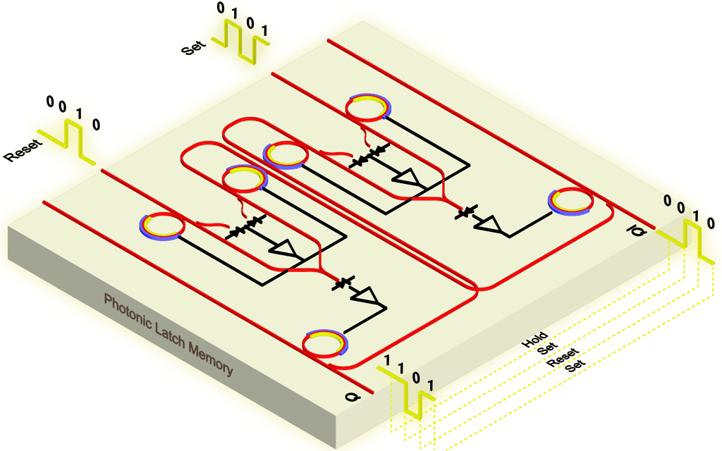
In a bid to accelerate processing speeds and efficiency in computationally intense applications such as artificial intelligence and sensing, researchers have developed a novel optical memory unit called a programmable photonic latch. This fast and scalable volatile photonic memory enables temporary data storage in optical processing systems, offering a high-speed solution using silicon photonics. By bridging the gap between optical communications and computing, this innovation has the potential to revolutionize the way we process and store data, paving the way for faster and more efficient systems.
Advancing Optical Memory Technology for Faster Processing Speeds
Researchers have made a significant breakthrough in developing a new type of optical memory unit called a programmable photonic latch, which is fast and scalable. This fundamental memory unit enables temporary data storage in optical processing systems, offering a high-speed solution for volatile memory using silicon photonics.
The new integrated photonic latch is modeled after a set-reset latch, a basic memory device used in electronic devices to store a single bit by switching between set (1) and reset (0) states based on inputs. This approach allows for fast optical data storage and retrieval, making it suitable for computationally intense applications such as artificial intelligence, sensing, and optical processing systems.
The researchers demonstrated the photonic latch using a programmable silicon photonic platform, showcasing its features such as optical set and reset, complementary outputs, scalability, and compatibility with wavelength division multiplexing (WDM). These characteristics make this approach promising for faster and more efficient optical processing systems.
Overcoming Challenges in Optical Memory
Optical technologies have been instrumental in advancing communication systems, but data storage remains predominantly electronic due to its scalability, compactness, and cost-effectiveness. However, transferring optical data to electronic memory – and back – increases energy consumption and introduces latency. Most existing optical memory implementations rely on bulky, costly, and energy-intensive setups or specialized materials that are not typically offered in commercially available silicon photonic processes.
To overcome these challenges, the researchers created an integrated programmable photonic latch based on optical universal logic gates using silicon photonic micro-ring modulators. These devices can be implemented in commercially available silicon photonic chip fabrication processes, making them scalable and fast.
Scalability and Wavelength Selectivity
One key advantage of the new system is its scalability. Because each memory unit has an independent input light source, it is possible to have several memory units working independently without affecting each other through optical power loss propagation. The memory units can also be co-designed with existing silicon photonic systems and built reliably with very high yields.
Another advantage is the photonic memory unit’s wavelength selectivity, which allows it to work seamlessly with WDM. This enables multi-bit data storage within a single memory unit and fast memory response time, measured in tens of picoseconds, outpacing the clock speeds of advanced digital systems and supporting high-speed optical data storage.
Future Research Directions
The researchers plan to pursue several research directions to make the new memory units more practical. This includes scaling the technology to a larger number of memory units and fabricating dedicated photonic memory chips. They also aim to develop a way to use a single manufacturing process to integrate both the photonic memory circuit and the electronics needed to control it.
By advancing optical memory technology, researchers can unlock faster processing speeds and more efficient data storage solutions for various applications. This breakthrough has the potential to revolutionize the field of optics and photonics, enabling new possibilities for scientific innovation and technological advancements.
External Link: Click Here For More


