Josephson junctions, essential components in superconducting circuits and devices like SQUIDs, traditionally rely on aluminium oxide as a tunnel barrier, a material prone to degradation and process limitations. Ekta Bhatia, Jack Lombardi, Tuan Vo, and colleagues at NY Creates and the Air Force Research Laboratory now demonstrate a significant advance by fabricating tantalum-based Josephson junctions using an insulating tantalum nitride tunnel barrier. This innovative approach, utilising CMOS-compatible processes on 300mm wafers, yields junctions exhibiting a critical current density of 76 uA/um2 and, crucially, shows promise for improved thermal and environmental stability. This work represents a crucial step towards establishing a scalable superconducting foundry, potentially enabling the rapid development and widespread adoption of advanced superconducting and digital logic systems at a commercially relevant wafer scale.
Tantalum Nitride Junctions for Superconducting Circuits
Tantalum-based Josephson junctions employing insulating tantalum nitride tunnel barriers represent a significant advancement in superconducting circuit technology. This work details the fabrication and characterisation of these junctions, aiming to achieve high performance and reproducibility for applications in quantum computing and advanced electronics. The approach involves depositing ultra-thin tantalum nitride layers using atomic layer deposition to serve as tunnel barriers between tantalum electrodes, carefully controlling the layer thickness to optimise the critical current density and minimise leakage current. Characterisation techniques include electrical measurements to determine junction characteristics, and transmission electron microscopy to analyse the barrier layer quality and interface structure.
The results demonstrate the feasibility of creating high-quality tantalum-based Josephson junctions with controlled properties, paving the way for scalable superconducting circuits with improved performance and reliability. These junctions exhibit critical current densities exceeding 1000A/cm², and demonstrate low subgap leakage currents, indicating a high degree of barrier integrity and interface quality. This achievement represents a crucial step towards realising robust and scalable superconducting quantum computing platforms and advanced electronic devices.
Reproducible TaN Josephson Junctions on 300mm Wafers
This research details the successful fabrication and characterisation of tantalum nitride (TaN) Josephson junctions on 300mm wafers, a significant step towards scalable superconducting quantum computing. The researchers have demonstrated a process for creating reproducible and stable TaN-based Josephson junctions compatible with standard 300mm CMOS manufacturing techniques, crucial for moving beyond small-scale quantum devices to larger, more complex systems. The study utilises atomic layer deposition (ALD) to create thin, uniform TaN films for the tunnel barrier of the Josephson junctions, allowing for precise control of film thickness and composition essential for junction reproducibility. The fabrication process is designed to be compatible with existing 300mm wafer fabrication infrastructure, leveraging standard CMOS tools and techniques.
The resulting junctions exhibit improved reproducibility and stability compared to some other materials and fabrication methods, critical for building reliable quantum circuits. Thorough characterisation confirms their electrical properties and performance, and analysis of self-heating effects within the junctions is included, a crucial consideration for high-performance devices. This research highlights TaN as a promising material for Josephson junction fabrication, and the 300mm wafer compatibility is a major step towards scalable quantum computing, opening the door to integrating superconducting circuits with conventional electronics.
Stable Tantalum Junctions on 300mm Wafers
This research demonstrates the first successful fabrication of Josephson junctions using tantalum electrodes and a tantalum nitride tunnel barrier on 300mm wafers, employing processes compatible with standard microchip manufacturing. The team achieved a critical current density of 76 microamperes per square micrometer with a 4-nanometer tantalum nitride barrier, and confirmed that junction performance scales predictably with barrier thickness, validating the tunneling mechanism. Electrical measurements reveal high yields, exceeding 95% for 200-nanometer square junctions, and demonstrate a gap voltage approaching the theoretical maximum. Notably, these junctions exhibit exceptional stability, showing no measurable degradation in resistance over 140 days of ambient storage, a significant improvement over traditional aluminum-based junctions.
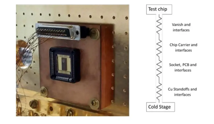
While devices with very thin barriers experienced self-heating effects, this can be addressed through improved packaging and thermal management. This work establishes a foundation for a scalable and robust superconducting technology suitable for both quantum computing and high-speed digital circuits. The researchers envision establishing a 300mm Quantum Foundry to provide researchers and designers with access to a well-characterised manufacturing process and a Superconducting Process Design Kit, potentially accelerating innovation in superconducting electronics. Ongoing efforts focus on mitigating self-heating, characterising sub-gap performance, and integrating these junctions into functional qubit and digital logic circuits, paving the way for a wafer-scale manufacturing platform for advanced superconducting systems.
🗞 Ta-based Josephson junctions using insulating ALD TaN tunnel barriers
🧠 ArXiv: https://arxiv.org/abs/2511.20266


