Elemental antimony holds considerable promise for next-generation phase-change memory and nanophotonic devices, owing to its simple composition and potential for high performance. Hanyi Zhang, Xueqi Xing, and Jiang-Jing Wang, alongside their colleagues, investigate the behaviour of antimony at the atomic level as its thickness shrinks to just a few nanometres. Their work reveals how reducing the film thickness impacts its optical properties, specifically demonstrating a reduction in both light absorption and the contrast between its different structural states. This research establishes a fundamental thickness limit of two nanometres for practical applications, and importantly, demonstrates that ultra-thin films exhibit enhanced stability, paving the way for robust and reversible optical switching in silicon-based devices.
Antimony Thin Film Properties via Density Functional Theory
Scientists systematically investigated the optical properties of antimony thin films, aiming to understand how thickness influences performance in phase-change memory and nanophotonic devices. The study employed density functional theory calculations alongside structural and optical experiments to explore films ranging from sub-nanometer to approximately 5. 1 nanometers in thickness. Researchers constructed a series of crystalline antimony models, building “slabs” by adding vacuum layers to hexagonal unit cells, creating structures from one bilayer up to 14 bilayers, corresponding to thicknesses of roughly 0.
27 to 3. 78 nanometers. This allowed for detailed analysis of how lattice parameters changed as the films were scaled down, revealing a consistent reduction in the in-plane lattice parameter from 0. 436nm in bulk antimony to 0. 412nm in the thinnest films, a phenomenon also observed in Raman spectroscopy experiments.
To model the amorphous phase, scientists generated melt-quenched amorphous antimony bulk models using atomistic simulations, then constructed slab models mirroring the thicknesses of the crystalline structures. Creating the thinnest amorphous model proved challenging, as antimony atoms tended to cluster laterally, but thicker models were built by combining multiple sub-slabs from different bulk amorphous models, ensuring smooth interfaces through relaxation processes. The team then calculated the density of states for both crystalline and amorphous models, revealing that a sizable energy gap persisted in crystalline films up to two bilayers and in amorphous films up to four bilayers, but diminished in thicker structures. These calculations, combined with structural characterization experiments, enabled the team to predict a bottom thickness limit of approximately 2 nanometers for functional antimony waveguide devices, corresponding to just 12 atomic layers in the crystalline phase.,.
Antimony Thin Films Show 2nm Thickness Limit
Scientists achieved a detailed understanding of the optical properties of antimony thin films, revealing a critical thickness limit for nanophotonic applications. The research demonstrates that as film thickness decreases, both the refractive index and extinction coefficient diminish, particularly in the near-infrared spectrum. Experiments revealed a bottom thickness limit of approximately 2 nanometers, corresponding to only 12 atomic layers in the crystalline phase, below which performance is significantly degraded. The team constructed a series of crystalline and amorphous antimony models, ranging from a single atomic layer up to 5.
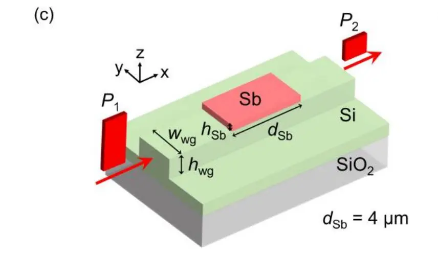
1 nanometers, to investigate these effects. Calculations of the dielectric function were performed for each model, accurately predicting the observed thickness-dependent trends in both refractive index and extinction coefficient. Spectroscopic ellipsometry experiments on antimony films ranging from 3 to 12 nanometers confirmed these predictions, demonstrating a clear reduction in the extinction coefficient as thickness decreased. These findings confirm the 2-nanometer thickness limit and demonstrate that even at this minimal thickness, the antimony films retain sizable contrast in physical properties, sufficient for practical phase-change applications. The improved amorphous-phase stability of the 2-nanometer films enables robust and reversible optical switching in silicon-based waveguide devices, paving the way for advanced nanophotonic technologies.,.
Antimony Film Thickness Limits Optical Performance
This research delivers a detailed understanding of how reducing the thickness of antimony films impacts their optical properties, crucial for applications like phase-change memory and nanophotonics. Through a combination of atomic-scale simulations and experimental validation, scientists determined that decreasing film thickness reduces both the extinction coefficient and optical contrast in the near-infrared spectrum. These changes establish a lower thickness limit of approximately 2 nanometers for effective performance in photonic devices, a prediction confirmed by both computational modelling and structural characterization. The team’s investigations reveal that the behaviour of amorphous and crystalline antimony differs as the film becomes thinner, impacting optical contrast.
Importantly, the study demonstrates that a 2-nanometer antimony film exhibits significantly improved stability in its amorphous phase, enabling robust and reversible optical switching within a silicon-based waveguide device. The researchers highlight antimony’s unique balance between crystallization kinetics and property contrast as the reason it remains the only successfully realized monatomic phase-change material. This work establishes a clear pathway for optimising material thickness in nonvolatile and reconfigurable optical applications, starting from fundamental atomic-scale principles.
👉 More information
🗞 Atomistic understanding of two-dimensional monatomic phase-change material for non-volatile optical applications
🧠 ArXiv: https://arxiv.org/abs/2512.10469


