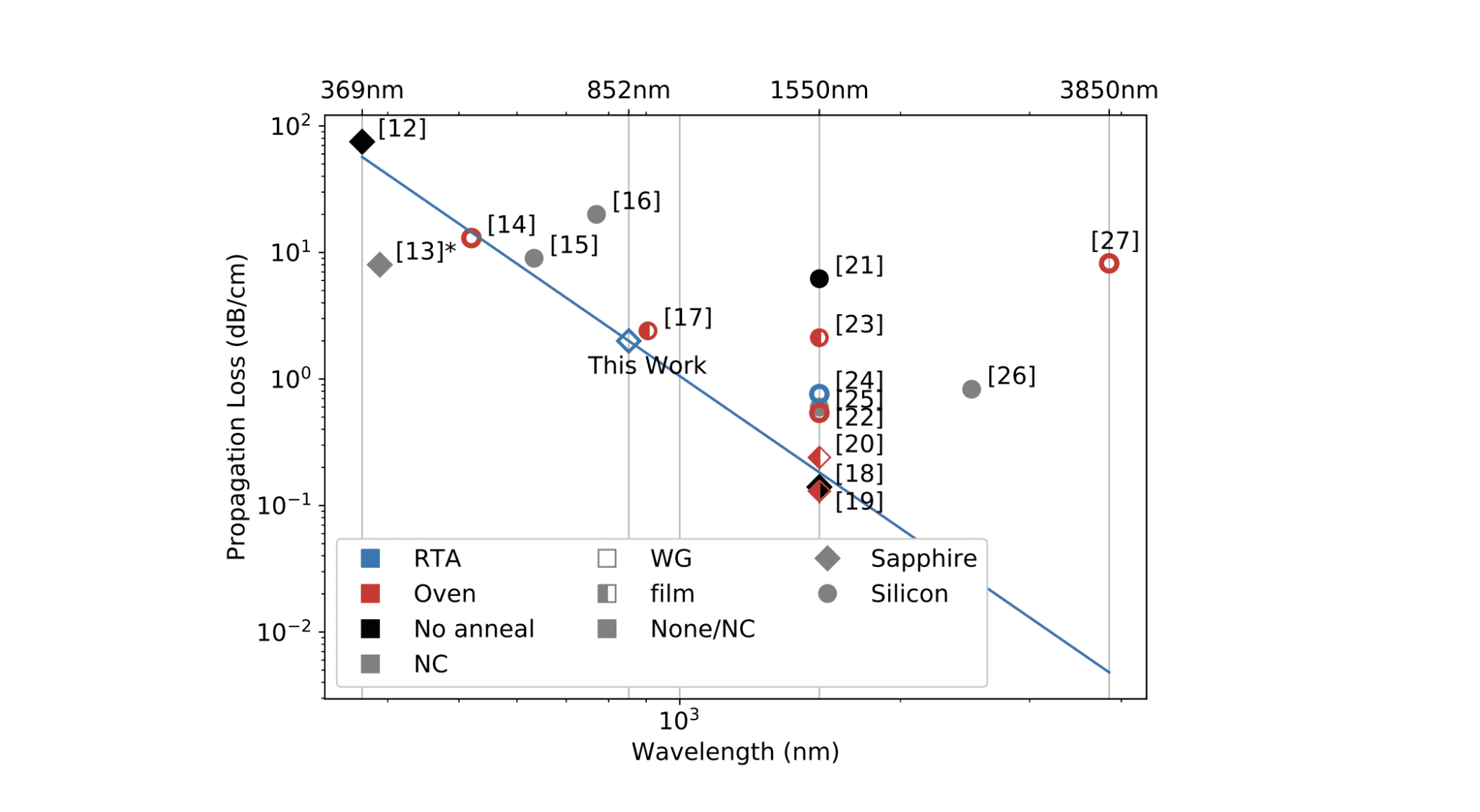
Aluminum nitride is rapidly becoming a key material for building miniature photonic circuits, particularly those operating with visible and ultraviolet light and potentially enabling advanced quantum technologies, but creating these circuits with minimal signal loss remains a significant hurdle. Nikolay Videnov, Matthew L. Day, and Michal Bajcsy, from the Institute for Quantum Computing, now demonstrate a fabrication process that dramatically reduces these losses in aluminum nitride waveguides. The team achieves a record low propagation loss of 2 decibels per centimetre at 852 nanometres, a substantial improvement enabled by carefully optimising each step of the manufacturing process. This work, which details the application of atomic layer deposition for surface protection and a subsequent rapid thermal anneal, represents a major step forward in realising practical, low-loss photonic circuits based on aluminum nitride.
Visible and ultraviolet light are essential for quantum technologies and other applications, and aluminum nitride (AlN) is emerging as a promising material for guiding these wavelengths. Achieving low light loss in AlN waveguides, however, remains a significant challenge, particularly at shorter wavelengths where light scattering increases. Researchers have now developed a detailed and reproducible fabrication process for low-loss AlN waveguides on sapphire, demonstrating a record propagation loss of only 2. 0±0. 3 decibels per centimeter at 852 nanometers.
Aluminum Nitride Waveguides for Integrated Photonics
This research details the fabrication and optimization of aluminum nitride (AlN) waveguides on sapphire for integrated photonics, with a focus on achieving ultralow loss and developing efficient electro-optic modulators. AlN was chosen for its high refractive index, transparency across a wide spectrum, and potential for strong interaction with light, while sapphire provides a stable substrate with excellent thermal conductivity. The team successfully created low-loss waveguides and efficient electro-optic modulators for photonic circuits operating in the near-infrared and visible spectrum. The fabrication process involves depositing AlN films on sapphire using techniques like sputtering or atomic layer deposition.
Electron beam lithography precisely defines the waveguide patterns, followed by reactive ion etching to create the waveguide structures. Atomic layer deposition of materials like silicon nitride passivates the waveguides, reducing surface roughness. Several techniques minimize propagation losses, including optimizing film deposition for dense, smooth AlN films and carefully controlling surface roughness with passivation layers, alongside careful design of waveguide geometry to minimize light confinement losses. The team employed a push-pull modulator configuration to enhance modulation efficiency and explored the electro-optic coefficient of AlN to optimize modulator performance. Rapid thermal annealing further refined the waveguide structure, potentially improving film density and reducing stress. The research confirms AlN on sapphire as a viable platform for integrated photonics, particularly for applications requiring low loss and efficient electro-optic modulation, opening possibilities in optical communications, sensing, quantum photonics, and biophotonics.
Low-Loss AlN Waveguides Fabricated on Sapphire
Aluminum nitride (AlN) is rapidly becoming a leading material for integrated photonics, particularly for applications requiring ultraviolet and visible light, such as trapped atom quantum technologies and underwater LIDAR. However, creating AlN waveguides with minimal light loss has proven challenging, especially at shorter wavelengths where light scattering significantly increases. Researchers have now demonstrated a detailed fabrication process for low-loss AlN waveguides on sapphire substrates, achieving a record propagation loss of only 2. 0±0. 3 decibels per centimeter at 852 nanometers.
This breakthrough represents a substantial improvement over previously reported losses at this wavelength and establishes a new benchmark for performance across the broader spectrum. The team’s success stems from a systematic optimization of the fabrication process, beginning with high-resolution electron beam lithography incorporating shape-based proximity effect correction. This precise patterning was followed by atomic layer deposition of aluminum oxide to passivate the waveguide surface, reducing surface defects that contribute to light scattering. Crucially, the researchers also implemented post-fabrication rapid thermal annealing, further refining the waveguide structure and minimizing loss.
Detailed analysis reveals that sidewall roughness introduced during fabrication is the primary source of loss, with material absorption negligible due to the high quality of the AlN films and the operating wavelength. The team’s approach focuses on minimizing scattering losses, which are particularly problematic at shorter wavelengths. By addressing sidewall roughness and employing high-quality materials, the researchers have created waveguides that exhibit exceptional performance and pave the way for more efficient and compact photonic devices operating in the ultraviolet and visible spectrum, promising to accelerate progress in diverse fields from quantum information processing to advanced imaging technologies.
Low-Loss AlN Waveguides on Sapphire Demonstrated
This work demonstrates a reproducible fabrication process for aluminum nitride (AlN) waveguides on sapphire, achieving a propagation loss of 2 decibels per centimeter at 852 nanometers, a record low for this material. This improvement stems from systematic optimization of several key techniques, including high-resolution electron beam lithography, atomic layer deposition for surface passivation, and a post-fabrication rapid thermal anneal. The researchers meticulously studied the contribution of each step, confirming that these combined methods significantly reduce light loss within the waveguides. The findings indicate that Rayleigh scattering currently limits performance in the best-performing waveguides, rather than material absorption. Importantly, the team found no benefit from using higher-grade AlN templates, suggesting that material quality is currently secondary to fabrication techniques in minimizing loss. While sapphire substrates yielded the lowest losses in this study, the results also show that silicon substrates can achieve good performance, offering additional advantages for integrated photonic circuits.
👉 More information
🗞 Low Loss Aluminum Nitride Waveguide Fabrication: Propagation Loss Reduction Through ALD and RTA
🧠 ArXiv: https://arxiv.org/abs/2508.20245


