Molybdenum disulfide, a material with great potential for next-generation electronics and photonics, undergoes a fascinating change as its layers stack, transitioning from a direct to an indirect band gap. Shunsuke Hirai, Ibuki Terada, and Michi-To Suzuki, from Osaka Metropolitan University and Osaka University, investigate the underlying cause of this shift using advanced computational modelling. Their work clarifies that the electronic behaviour isn’t solely determined by atomic orbitals pointing outwards from the layers, but crucially involves contributions from orbitals lying within the plane of the material. This discovery provides a more complete understanding of how to control the electronic properties of molybdenum disulfide, paving the way for improved design and performance in future devices.
considerable attention as a promising alternative to graphene for applications in field-effect transistors and nanophotonic devices because of its sizable band gap, high carrier mobility, large on/off ratio, and strong photoluminescence efficiency. A particularly intriguing property of MoS2 is the transition of its band gap character with layer thickness; while the monolayer exhibits a direct gap, the band gap becomes indirect in multilayer and bulk forms. To clarify the microscopic mechanism behind this transition, the researchers performed first-principles calculations combined with Wannier-based modeling, focusing on the roles of atomic orbitals and interlayer interactions. The work investigates how orbitals oriented perpendicular to the layers contribute to the observed changes in the electronic structure of MoS2 as its thickness varies.
Band Gap Evolution in Layered Molybdenum Disulfide
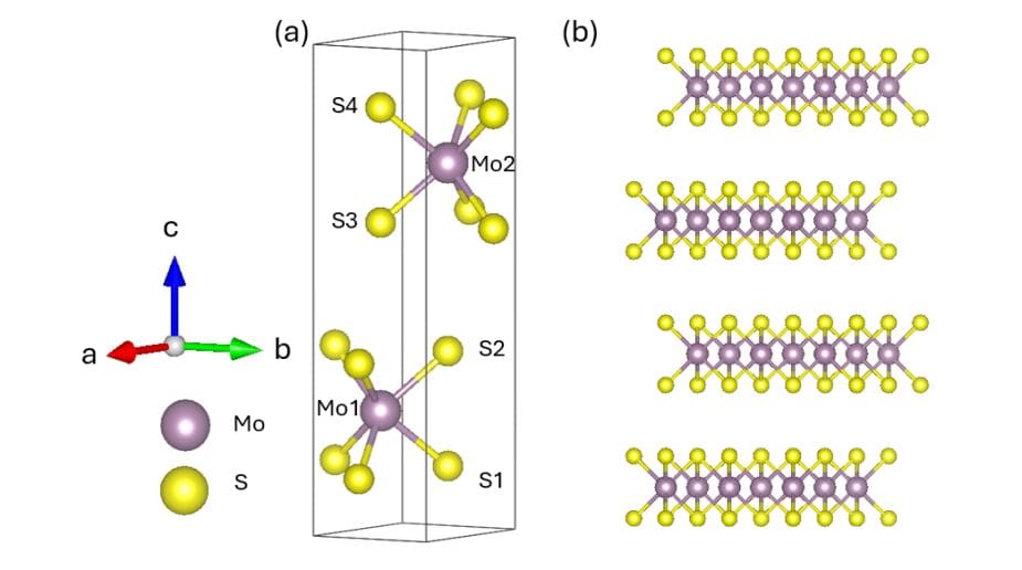
Scientists conducted a detailed investigation into the electronic structure of molybdenum disulfide (MoS2) to understand how its band gap changes with layer thickness, transitioning from a direct gap in single-layer material to an indirect gap in multilayer and bulk forms. The research focused on clarifying this transition by employing first-principles calculations combined with a sophisticated Wannier-based modeling approach to analyze the roles of atomic orbitals and interlayer interactions. Calculations accurately determined optimized lattice constants and internal atomic parameters, ensuring high accuracy in the modeling. To model multilayer systems, scientists constructed a tight-binding model based on the bulk electronic structure calculated with these advanced methods.
They selected molybdenum-4d and sulfur-3p orbitals as key components, recognizing their primary contribution to electronic states near the Fermi level. A Hamiltonian was then constructed for systems with varying numbers of layers, incorporating both intralayer and interlayer interactions, and accurately representing the multilayer structure. This approach allowed the team to investigate the evolution of the band structure as the number of layers increased, providing insights into the fundamental physics governing the direct-to-indirect band gap transition. The team validated their model by demonstrating strong agreement between tight-binding model results and the initial calculations for bulk MoS2.
MoS2 Layering Defines Band Gap Transition
Scientists have achieved a detailed understanding of how the electronic properties of molybdenum disulfide (MoS₂) change as its layers increase, transitioning from a direct to an indirect band gap. This work clarifies the fundamental mechanisms governing this transition, providing insights for engineering the band gap in layered materials for future devices. Researchers performed first-principles calculations and constructed a tight-binding model to analyze the roles of atomic orbitals and interlayer interactions in shaping the electronic band structure of MoS₂. The team’s calculations accurately reproduce the electronic bands around the energy gap in bulk MoS₂, demonstrating the model’s reliability.
Results show that monolayer MoS₂ exhibits a direct band gap of 1. 72 electron volts, while bulk MoS₂ has an indirect band gap of 0. 958 electron volts. Analysis of bilayer and 6-layer systems revealed that increasing the number of layers causes energy bands to shift and split, significantly modifying the overall band structure. Specifically, the team observed that band splitting varies depending on the location within the structure.
As the number of layers increases, the critical points defining the conduction and valence bands shift, causing changes in the valence-band top and conduction-band bottom. Further investigation revealed that specific orbitals contribute significantly to these changes. These findings demonstrate the crucial role of both out-of-plane and in-plane orbital contributions in governing the electronic structure of layered MoS₂, providing a foundation for precise band gap engineering in future van der Waals materials.
Sulfur Orbitals Drive Band Gap Transition
This research successfully clarifies the origins of changes in the electronic band structure of molybdenum disulfide, a material with potential for advanced electronic and photonic devices. Scientists employed detailed computational modeling to investigate how the arrangement of atomic orbitals contributes to the material’s band gap, revealing that the behavior of sulfur atoms plays a crucial role. The study demonstrates that while out-of-plane orbitals are significant, in-plane orbitals also contribute to interlayer interactions and modify the band gap characteristics. Specifically, the team found that the band gap transition from direct to indirect as the material layers increase is driven by changes in the sulfur p orbitals, rather than the molybdenum orbitals previously thought to be dominant.
The magnitude of band splitting, which dictates the material’s electronic properties, is determined by the interplay between these orbitals and their interactions between layers. This detailed understanding of orbital contributions provides a foundation for engineering the band structure of molybdenum disulfide and optimizing its performance in future devices. This work provides a detailed atomic-level understanding of the material’s behavior, paving the way for targeted design of materials with tailored electronic characteristics.
👉 More information
🗞 Wannier based analysis of the direct-indirect bandgap transition by stacking MoS layers
🧠 ArXiv: https://arxiv.org/abs/2511.15178


