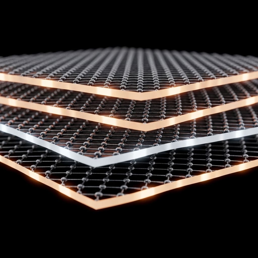
Researchers are increasingly focused on harnessing correlated insulating behaviour in graphene to unlock emergent phenomena such as superconductivity and magnetism. Xinyu Cai, Fengfan Ren, and Qiao Li, all from ShanghaiTech University, alongside Yanran Shi, Yifan Wang, Yifan Zhang, Zhenghang Zhi, Jiawei Luo, Yulin Chen, and Jianpeng Liu, also of ShanghaiTech University, working with Xufeng Kou and Zhongkai Liu, demonstrate a new method for achieving this using bilayer graphene. Their work details the creation of an artificial Kagome superlattice through nanopatterning of the substrate, offering a precisely defined and tunable periodic potential. This approach overcomes reproducibility and tunability issues associated with traditional moiré graphene superlattices, revealing a stack of correlated insulating states and establishing dielectric-patterned graphene superlattices as a robust platform for exploring flat-band-induced correlated phenomena.
Imagine building a miniature city with perfectly arranged blocks, controlling how electrons flow through it. That level of precision is now possible with bilayer graphene, creating multiple, interacting layers of insulating behaviour. This new technique offers a reliable route to harnessing strong electron interactions for future electronic devices. Scientists have long sought to control the behaviour of electrons in materials to create new quantum phenomena.
Graphene, a single-atom-thick sheet of carbon, presents a particularly promising platform due to its exceptional electronic properties. Recent work has focused on engineering ‘flat bands’ within graphene’s electronic structure, where electrons experience reduced kinetic energy and enhanced interactions, potentially leading to states like superconductivity and correlated insulation.
Achieving these flat bands has traditionally relied on creating moiré superlattices, patterns arising from the slight misalignment of graphene layers, or utilising specific stacking arrangements. However, these methods often suffer from inconsistencies in fabrication and limited control over the resulting electronic properties. Researchers have now introduced a new approach: an artificial Kagome superlattice in bilayer graphene.
This structure is created by precisely nanopatterning a dielectric substrate, effectively imposing a periodic potential onto the graphene. Unlike previous techniques, this method offers a high degree of control over the superlattice’s characteristics, including its period and symmetry. Magnetotransport measurements performed on these devices reveal the emergence of multiple correlated insulating states at moderate superlattice potentials.
These states, indicative of strong electron-electron interactions within the Kagome-induced flat bands, diminish as temperature increases, suggesting a thermally driven suppression of these interaction-driven phenomena. Detailed continuum-model calculations corroborate these experimental findings, confirming the formation of multiple flat minibands and accurately reproducing the observed changes in the band structure.
These results demonstrate that dielectric-patterned graphene superlattices represent a dependable and adjustable architecture for realising flat-band-induced correlated phenomena, extending possibilities beyond conventional moiré systems. Once a material’s electrons are confined to flat bands, their interactions become dominant, potentially giving rise to exotic quantum states.
Realising these flat bands has proven challenging. Existing methods, such as creating moiré superlattices by twisting graphene layers or using specific stacking arrangements, often lack the precision and tunability needed for detailed studies. A new strategy, artificially engineering superlattices, offers a potential solution. By carefully patterning a substrate, scientists can create a periodic potential that mimics the effects of moiré patterns while maintaining greater control over the superlattice’s properties.
Kagome lattices, characterised by a network of corner-sharing triangles, are particularly interesting due to their geometrical frustration, which can lead to flat bands and a variety of correlated and topological phases. Initial attempts to create artificial Kagome superlattices in monolayer graphene have shown promise in manipulating Dirac fermions, but conclusive evidence of strong electron-electron interactions and correlated quantum phases has been lacking.
Researchers turned to bilayer graphene, where the parabolic low-energy bands allow a Kagome superlattice to more efficiently suppress electron motion, creating flatter and more isolated minibands. Applying an external electric field can open and tune a band gap, further enhancing the interaction-driven correlated states. A bilayer graphene Kagome superlattice was constructed via nanopatterning of a dielectric substrate, ensuring high reproducibility, tunable lattice symmetry, and minimal disorder.
By systematically adjusting the superlattice potential, band-structure modulation was observed, most in particular the emergence of a stack of correlated insulating states associated with Kagome-induced flat bands. These correlated states disappear at higher temperatures as the interaction-driven gap closes, a finding supported by continuum-model calculations that accurately capture the formation of multiple flat minibands and the evolution of the band structure. This work establishes the BLG Kagome superlattice as a strong and tunable architecture for exploring correlated phases in a controlled environment, opening new avenues beyond moiré-based systems.
Fabrication of bilayer graphene Kagome superlattices via electron-beam lithography and dielectric patterning
Researchers fabricated bilayer graphene Kagome superlattice devices for transport measurements, beginning with a precisely defined Kagome pattern etched onto a silicon dioxide substrate using high-precision electron-beam lithography and subsequent reactive ion etching. The resulting array of dielectric holes possessed an average nearest-neighbour spacing of 52nm, establishing a Kagome lattice constant of 104nm.
To maintain device integrity and minimise disorder, a thin hexagonal boron nitride flake, less than 5nm thick, was inserted between the patterned dielectric and the bilayer graphene. Dual gating was implemented using a graphite top gate and a silicon back gate, affording independent control over both carrier density and the superlattice potential. Atomic force microscopy confirmed the uniformity and periodicity of the etched Kagome lattice, revealing consistently distributed holes and clean surfaces, which is vital for a well-defined superlattice potential.
A global back-gate voltage applied through the silicon substrate induced a periodic superlattice potential within the bilayer graphene. Numerical simulations of the potential profile at a back-gate voltage of -20V demonstrated that the electrostatic potential within the etched holes was approximately 0.3V lower than the surrounding areas, thereby establishing the characteristic Kagome superlattice potential.
By systematically varying the superlattice potential, the band structure of the bilayer graphene was modulated, allowing for the observation of correlated insulating states. Unlike previous approaches relying on twist-angle inhomogeneity or rhombohedral stacking, this method prioritises reproducibility, tunability, and scalability, offering a high-quality platform for investigating exotic correlated phenomena. This dielectric-patterned approach provides a means to explore flat-band-induced correlated phenomena beyond the limitations of moiré superlattices.
Kagome superlattice potential induces correlated insulating states and thermal gap collapse
At moderate superlattice potentials, magnetotransport measurements revealed the emergence of a stack of correlated insulating states, characteristic of strong electron-electron interactions within Kagome-induced flat bands. Increasing temperature caused these correlated gaps to collapse, demonstrating the thermal suppression of interaction-driven states.
Continuum-model calculations confirmed the formation of multiple flat minibands and accurately reproduced the observed evolution of band reconstruction. Detailed analysis of the band structure modulation showed that the Kagome superlattice potential effectively alters the electronic properties of bilayer graphene. Numerical simulations indicated that the electrostatic potential within the etched holes is approximately 0.3V lower than the surrounding regions at a back-gate voltage of -20V.
This establishes a characteristic Kagome superlattice potential, important for inducing the observed correlated behaviour. Low-temperature transport measurements were performed to probe the resulting band structure. The observed correlated insulating states are not merely a static feature. At 2K, clear signatures of these states were present, but as temperature rose to 5K, the insulating gaps began to diminish.
By 10K, the gaps had collapsed, demonstrating the delicate balance between electron interactions and thermal energy. The calculations also reproduced the evolution of these bands as the superlattice potential was tuned. At a lattice constant of 104nm and a nearest-neighbour spacing of 52nm, the fabricated Kagome pattern exhibited excellent uniformity. AFM characterisation confirmed this structural homogeneity, with uniformly distributed holes and clean surfaces.
This high degree of order is vital for establishing a well-defined superlattice potential in the bilayer graphene. Previous moiré superlattice approaches often suffer from twist-angle inhomogeneity and structural relaxation.
Nanopatterned graphene substrates induce tunable correlated insulating states
Scientists have long sought to engineer materials where electrons behave in unusual ways, hoping to unlock new technologies. Recent work with bilayer graphene, patterned with a precise artificial lattice, represents a step forward in controlling these electron interactions. For years, creating genuinely flat energy bands, essential for observing these interactions, depended on chance alignments in twisted layers of graphene or specific stacking arrangements, both notoriously difficult to produce consistently.
This new approach bypasses those limitations by directly sculpting the material’s environment. Researchers created a periodic potential using nanopatterning of the substrate beneath the graphene. By altering an applied voltage, they can tune the electronic properties with unprecedented control. Observations reveal the emergence of multiple correlated insulating states, where electrons collectively resist the flow of current, a behaviour linked to the flat bands created by the artificial lattice.
Increasing the temperature weakens these states, demonstrating the delicate balance between electron interactions and thermal energy. Flat bands are becoming increasingly accessible for experimental study. Maintaining these delicate states requires very low temperatures, restricting immediate practical applications. The ability to create and adjust these flat bands opens possibilities beyond simple electronic devices.
This work suggests a path toward designing materials with tailored electronic properties, potentially leading to new types of sensors or even components for quantum computing. This technique offers a reliable and adjustable platform for exploring correlated electron phenomena. This means a shift from relying on serendipitous discoveries to a more systematic approach to material design.
The patterned dielectric approach is scalable, future efforts might focus on integrating these structures into more complex devices. A key question remains: can these engineered states be made stable at higher temperatures, bringing the promise of flat-band physics closer to real-world applications.
👉 More information
🗞 Stack of correlated insulating states in bilayer graphene kagome superlattice
🧠 ArXiv: https://arxiv.org/abs/2602.16210


