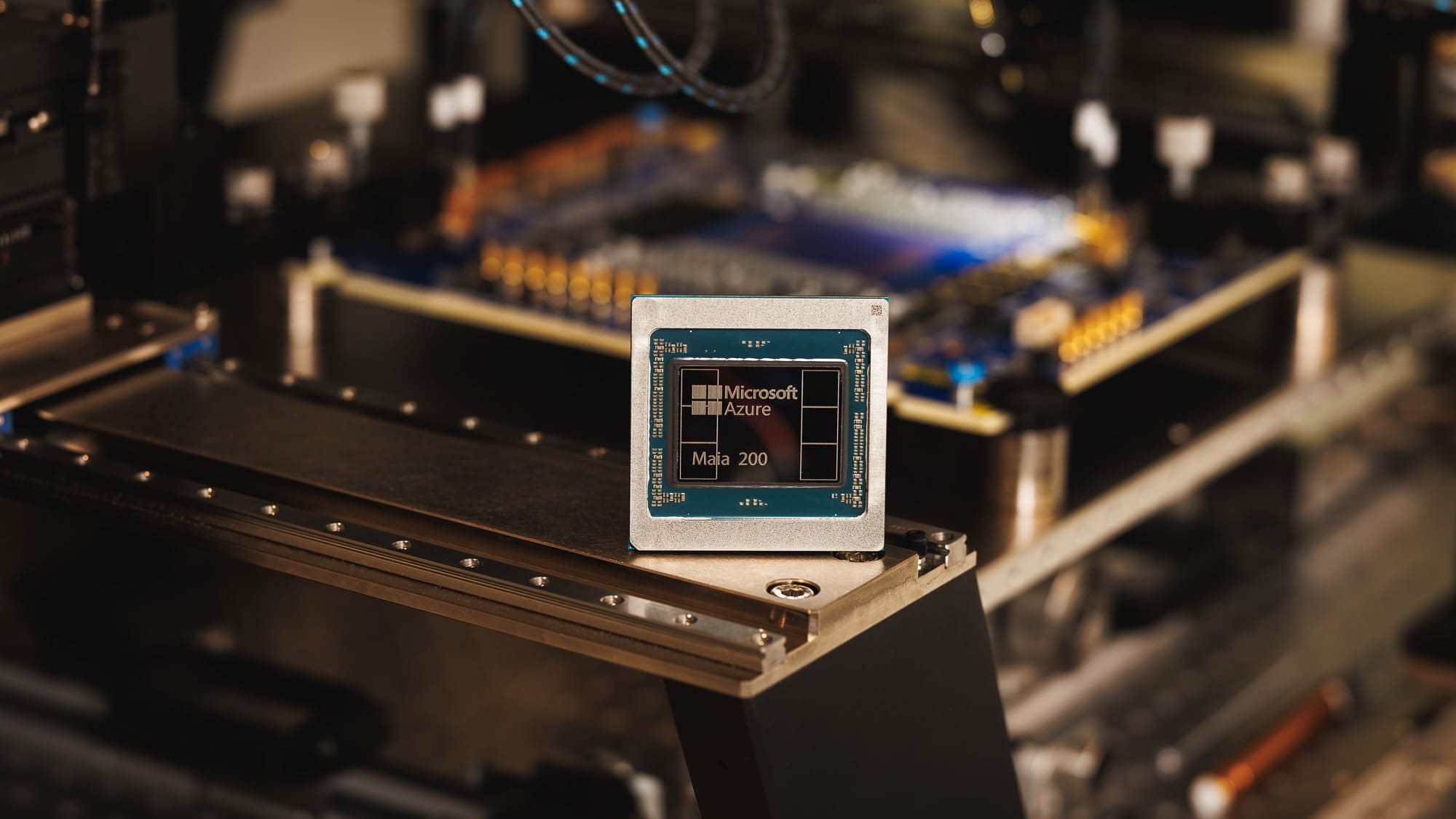
Microsoft has unveiled Maia 200, a groundbreaking AI inference accelerator poised to redefine the economics of AI token generation. Engineered on TSMC’s cutting-edge 3nm process, the Maia 200 boasts 216GB of HBM3e memory and delivers a staggering three times the FP4 performance of Amazon’s Trainium and superior FP8 performance to Google’s latest TPU. “Today, we’re proud to introduce Maia 200, a breakthrough inference accelerator,” said Scott Guthrie, Executive Vice President, Cloud + AI. This first-party silicon will power demanding applications like OpenAI’s GPT-5.2 models within Microsoft Foundry and Copilot, and represents a 30% performance-per-dollar improvement over Microsoft’s current hardware—marking a significant leap forward in efficient AI infrastructure.
TSMC 3nm Process & 216GB HBM3e Memory Architecture
Microsoft’s newly unveiled Maia 200 AI inference accelerator leverages leading-edge fabrication techniques to achieve substantial performance gains. The chip is built on TSMC’s 3nm process, incorporating over 140 billion transistors within a 750W SoC TDP envelope, optimized for large-scale AI workloads and efficient power consumption. This advanced process allows Maia 200 to deliver over 10 petaFLOPS in 4-bit precision (FP4) and over 5 petaFLOPS of 8-bit (FP8) performance. Beyond transistor count, the architecture prioritizes data handling, recognizing that “FLOPS aren’t the only ingredient for faster AI. Feeding data is equally important.”
A critical component of this performance is a redesigned memory subsystem centered around 216GB of HBM3e memory operating at 7 TB/s. This isn’t simply about capacity; the system employs a specialized DMA engine, on-die SRAM, and a novel NoC fabric to maximize token throughput. The design is specifically tuned for narrow-precision datatypes, further accelerating AI inference tasks. Furthermore, the Maia 200 incorporates a unique two-tier scale-up network, utilizing standard Ethernet alongside a custom transport layer, achieving 2.8 TB/s of bidirectional, dedicated scaleup bandwidth. “Each accelerator exposes…predictable, high-performance collective operations across clusters of up to 6,144 accelerators,” ensuring scalable performance and reduced power usage across Azure’s infrastructure. Within each rack, four Maia accelerators connect via direct links, minimizing latency, while the same communication protocols extend to inter-rack networking, simplifying programming and maximizing efficiency. Microsoft’s approach to validation, utilizing a sophisticated pre-silicon environment, allowed for optimization of silicon, networking, and software concurrently, resulting in AI models running on Maia 200 silicon “within days of first packaged part arrival.” This holistic development process reduced time to datacenter rack deployment to less than half that of comparable programs.
Maia 200 Achieves 3x FP4 Performance Over Amazon Trainium
Microsoft’s newly unveiled Maia 200 is demonstrably outperforming competitor hardware in the critical area of AI inference, achieving three times the FP4 performance of Amazon’s third-generation Trainium chip. This leap in capability isn’t simply a matter of raw computational power, but a holistic design philosophy focused on efficient data handling. The accelerator, fabricated on TSMC’s 3nm process, incorporates over 140 billion transistors, and delivers over 10 petaFLOPS in 4-bit precision (FP4). A crucial element of this performance is the redesigned memory subsystem, specifically engineered to tackle the bottlenecks inherent in feeding massive AI models.
Microsoft emphasizes that “feeding data is equally important,” highlighting the integrated approach to both processing and data delivery. The architecture extends to the system level with a novel two-tier scale-up network built on standard Ethernet, promising both performance and cost advantages. Each accelerator can achieve 2.8 TB/s of bidirectional, dedicated scaleup bandwidth. “This gives developers fine-grained control when needed while enabling easy model porting across heterogeneous hardware accelerators,” according to Microsoft, who are previewing the Maia SDK to facilitate optimization and model building.
The Maia 200 is currently deployed in the US Central datacenter region near Des Moines, Iowa, with expansion planned to the US West 3 region near Phoenix, Arizona.
Maia 200 is an AI inference powerhouse: an accelerator built on TSMC’s 3nm process with native FP8/FP4 tensor cores, a redesigned memory system with 216GB HBM3e at 7 TB/s and 272MB of on-chip SRAM, plus data movement engines that keep massive models fed, fast and highly utilized.
Scott Guthrie
Two-Tier Scale-Up Network & Maia AI Transport Protocol
Microsoft is deploying a novel networking architecture alongside its Maia 200 AI accelerator, designed to overcome bottlenecks in large-scale AI inference. Four Maia accelerators are directly connected via non-switched links, minimizing latency for optimal inference. This same communication protocol, the “Maia AI transport protocol,” extends seamlessly from intra-rack to inter-rack networking, allowing for scaling “across nodes, racks and clusters of accelerators with minimal network hops.” Microsoft asserts this unified fabric simplifies programming and reduces wasted capacity, maintaining consistent performance while controlling costs at cloud scale.
A key element of Maia 200’s development was a “sophisticated pre-silicon environment” used to model LLM computation and communication patterns. This allowed the team to optimize the entire system—silicon, networking, and software—concurrently. Scott Guthrie notes that the company is already “designing for future generations” of the Maia accelerator, anticipating continual performance improvements.
Rapid Deployment Enabled by Pre-Silicon Validation & Azure Integration
Microsoft’s newly unveiled Maia 200 AI accelerator isn’t simply a feat of chip engineering; a core strategy focused on pre-silicon validation and seamless Azure integration dramatically accelerated its deployment. This proactive approach allowed for unified optimization of the silicon, networking, and system software “long before first silicon,” a departure from conventional development timelines. This comprehensive validation extended beyond the chip itself, with early work dedicated to critical system elements like the backend network and a second-generation liquid cooling system.
Native integration with the Azure control plane further streamlines operation, delivering crucial security, telemetry, diagnostics, and management capabilities at both chip and rack levels. Developers can now access the Maia SDK, a complete toolkit featuring PyTorch integration, a Triton compiler, and a low-level programming language, allowing for both fine-grained control and effortless model porting. Microsoft emphasizes that this holistic methodology—from chip design to software and datacenter implementation—directly translates to “higher utilization, faster time to production and sustained improvements in performance per dollar and per watt at cloud scale.”


