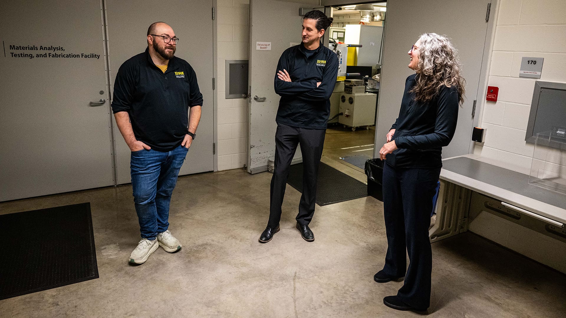
The University of Iowa secured $1.5 million to expand its materials science center and explore quantum technologies. The U.S. Department of Defense award will fund infrastructure improvements and new equipment at the university’s MATFab facility. This investment aims to unite researchers in investigating materials for light- or electronic-based quantum systems.
$1.5 Million DoD Award Fuels Quantum Materials Research
The $1,498,989 award from the U.S. Department of Defense will facilitate the acquisition of a maskless grayscale lithography system, capable of creating three-dimensional structures with a resolution down to 300 nanometers. This system will allow researchers to “draw” patterns with a laser, varying height from the surface, and then etch and stack materials for device fabrication. Researchers aim to optimize optical and electronic properties by creating layered materials, similar to a “nano-sandwich,” for use in quantum systems.
This investment will modernize the 1,500 square foot MATFab facility, established in 2019, by replacing dated equipment and expanding capabilities in heterogeneous material integration. The facility will serve as a regional innovation center, offering training to students and faculty from other Iowa colleges, and fostering collaborative projects focused on quantum technologies and applications like improved sensors and faster mapping. Researchers will study individual material properties at the micron and nanoscale to determine their potential in building compact devices.
MATFab Facility Expands Nanofabrication & Heterogeneous Integration
This capability supports the creation of layered structures—like a “nano-sandwich”—to optimize optical and electronic properties for quantum systems. The program will provide training on new materials fabrication tools, fostering collaborative projects and positioning MATFab as a central hub for advanced materials research.
Maskless Lithography Enables 300 Nanometer Resolution Patterning
A key component of the research enabled by the award is a maskless grayscale lithography system. This level of precision facilitates the creation of extremely fine details and patterns with varying heights on material surfaces. The lithography system is paired with etching tools and layering capabilities, allowing for the construction of complex, stacked materials. This process, described as building “nano-sandwiches,” is intended to optimize the optical and electronic properties of the materials for use in devices. Ultimately, this technology aims to move theoretical structures toward functional devices relevant to quantum technologies like light-routing systems and transistors.


