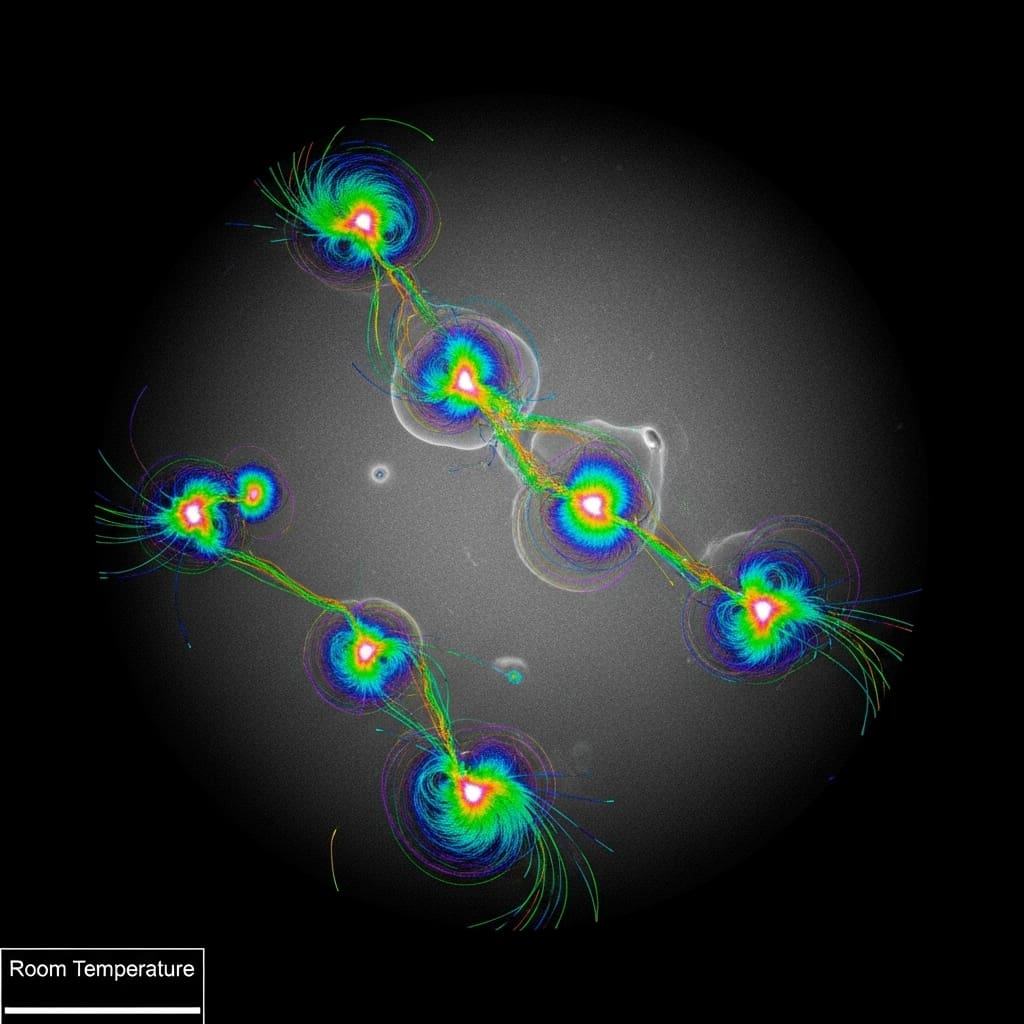
The performance of modern semiconductor devices hinges on understanding and controlling nanoscale defects, but pinpointing the origin of electrical noise at this level has remained a significant challenge. Jinpeng Liu, Yuanhong Teng, and Yu Chen, along with colleagues at institutions including Jun Yin’s group, now present a breakthrough in characterizing these defects within silicon carbide. They achieve real-time observation of single-charge movement in a commercial semiconductor at room temperature, a feat previously unattainable, by employing a novel technique that combines optical detection with magnetic resonance. This work not only reveals the dynamics of nanoscale charge defects but also establishes a new method for electrical noise imaging, offering crucial insights for improving silicon carbide fabrication and ultimately advancing semiconductor technology.
Silicon Carbide Defects Characterised by Quantum Noise Spectroscopy
Researchers investigate nanoscale charge defects within silicon carbide, employing quantum noise spectroscopy to characterise these imperfections at room temperature. This technique allows for the detection and analysis of individual defects without the need for cryogenic cooling, a significant advancement over previous methods. The team successfully resolves the spectral signatures of individual defects, revealing information about their energy levels and interactions with the surrounding environment, establishing a pathway for precise characterisation of defects in silicon carbide and paving the way for improved material quality and enhanced performance in quantum devices.
Silicon Carbide Quantum Sensors Detect Nanoscale Fields
Silicon carbide defects, specifically the PL5 center and silicon vacancies, function as highly sensitive quantum sensors at room temperature. These sensors achieve nanoscale resolution and sub-nanotesla magnetic field sensitivity, enabling measurements of various physical parameters including magnetic and electric fields. Researchers can determine the location of charge associated with the PL5 defect and have characterised noise sources limiting sensor coherence, developing methods to mitigate these effects. This technology has potential applications in magnetic resonance spectroscopy at the single-molecule level, material science, biological sensing, and quantum information processing.
Nanoscale Noise Imaging of Silicon Carbide
This research presents a new method for characterising semiconductor materials with nanoscale precision, utilising single PL5 centers in silicon carbide as broadband quantum sensors. Scientists observed, in real-time, the dynamics of single-charge tunneling within a commercial semiconductor at room temperature, a significant advancement in understanding noise sources at this scale. The technique enables electrical noise imaging, revealing variations across different wafer substrates and establishing a quantitative metric for assessing wafer quality, while analyses indicate the presence of silicon and carbon vacancies and interactions between defects, suggesting potential for creating hybrid qubit systems.
👉 More information
🗞 Quantum Noise Spectroscopy of Nanoscale Charge Defects in Silicon Carbide at Room Temperature
🧠 ArXiv: https://arxiv.org/abs/2512.22521


