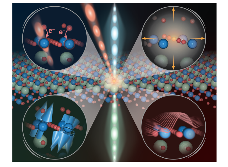
Understanding how energy flows and materials change at the nanoscale is fundamental to advances in quantum materials and sustainable energy technologies, and researchers are now employing increasingly sophisticated techniques to observe these processes directly. Wonseok Lee, Levi D. Palmer, and colleagues, including Thomas E. Gage from Argonne National Laboratory and Scott K. Cushing from the California Institute of Technology, are at the forefront of this field, having developed and refined time-resolved and ultrafast electron energy-loss spectroscopy. This technique allows scientists to image the behaviour of photoexcited carriers, lattice vibrations, and heat flow with unprecedented temporal and spatial resolution, spanning timescales from femtoseconds to microseconds. By combining theoretical advances with improvements in instrumentation, the team demonstrates how this powerful method reveals dynamic processes crucial to the design of next-generation materials and devices.
Time-resolved and ultrafast electron energy-loss spectroscopy represents an emerging technique for measuring photoexcited carriers, lattice dynamics, and near-fields across femtosecond to microsecond timescales. When performed in either a specialized scanning transmission electron microscope or ultrafast electron microscope, this technique directly images charge carriers, lattice vibrations, and heat dissipation following photoexcitation or applied bias. Recent advances in theoretical calculations and electron optics are enabling new capabilities, allowing researchers to probe the fundamental processes governing energy flow in materials with unprecedented temporal and spatial resolution. This approach offers a powerful means to understand the behaviour of complex materials and devices, bridging the gap between theoretical predictions and experimental observations, and promises to advance understanding of phenomena ranging from fundamental physics to materials science and nanotechnology.
Time-Resolved Microscopy with Ultrafast Electrons
The field of ultrafast electron microscopy requires expertise in physics, chemistry, materials science, and engineering. This technique uses short bursts of electrons to observe changes in materials at incredibly short timescales, revealing how energy flows and how materials respond to external stimuli. A key component is the generation of these short electron pulses, often achieved using lasers to liberate electrons from a material. Researchers continually refine the systems used to create and control these electron beams, addressing challenges such as minimizing sample damage. Synchronization between the laser pulse that initiates changes and the electron pulse used to observe those changes is also critical for achieving high temporal resolution.
UEM experiments often involve studying materials under realistic operating conditions, a technique known as in situ microscopy. This allows scientists to observe dynamic processes, such as chemical reactions or electrochemical processes, as they occur. The technique is also being applied to investigate the vibrations of atoms within a material, known as phonon dynamics, and to study the interaction of light and electrons in nanostructures. Significant progress has been made in developing platforms to aid in the establishment of UEM laboratories, making this powerful technique more accessible to researchers.
Ultrafast Spectroscopy Reveals Energy Loss Mechanisms
Time-resolved and ultrafast electron energy-loss spectroscopy provides a powerful means to investigate photoexcited carriers, lattice dynamics, and near-fields across timescales ranging from femtoseconds to microseconds. This technique directly images charge carriers, lattice vibrations, and heat dissipation within a specimen, revealing fundamental insights into material behavior. Measurements establish that when electrons interact with a sample, most pass through without losing energy, creating a strong signal. However, some electrons lose energy through interactions with the material, providing information about its composition and structure.
The energy lost by these electrons reveals a wealth of information, including details about atomic and lattice vibrations, the material’s band gap, and its dielectric properties. By analyzing the energy loss spectrum, researchers can determine the material’s thickness, valence electron density, and even the arrangement of atoms within the material. Photoexcitation alters the EEL spectrum through both local electromagnetic fields and changes in electron or phonon populations. Specifically, a local electromagnetic field modifies the electron probe, enabling ultrafast imaging of charge dynamics at nanometer spatial and femtosecond temporal resolutions. A key feature of this technique is the observation of “bulk plasmons,” collective oscillations of electrons within the material. Researchers have significantly refined both the theoretical calculations underpinning the interpretation of spectra and the instrumentation used to acquire them, extending the technique’s capabilities beyond traditional photon-induced near-field electron microscopy. These improvements allow for detailed investigation of dynamic processes occurring on femtosecond to microsecond timescales in a variety of materials. The study highlights the growing sophistication of methods for calculating and interpreting electron energy-loss spectra, encompassing both ground-state properties and transient behaviour following excitation.
Furthermore, the review details emerging hardware developments, including electron beam monochromation, in situ experimentation capabilities, and laser-free ultrafast electron microscopy, alongside high-speed direct electron detectors. While acknowledging current limitations in spatial resolution, the authors suggest these advancements position time-resolved and ultrafast electron energy-loss spectroscopy as a crucial tool for understanding nanoscale dynamics in quantum materials and solar energy conversion devices. Future work will likely focus on refining these hardware components and pushing the boundaries of achievable spatial and temporal resolution.
🗞 Imaging Nanoscale Carrier, Thermal, and Structural Dynamics with Time-Resolved and Ultrafast Electron Energy-Loss Spectroscopy
🧠 ArXiv: https://arxiv.org/abs/2510.05413


