Visualising electric fields at the nanoscale presents a significant challenge in materials science, but researchers are now achieving unprecedented clarity with a novel technique. Zhi Cheng, Zhiwei Yu, and Mengqi Wang, alongside colleagues, have developed a scanning method using nitrogen-vacancy centres in diamond that resolves electric fields with approximately 10 nanometre precision. This breakthrough overcomes limitations of previous approaches by employing a uniquely sensitive probe that maintains close contact with the sample while simultaneously minimising signal distortion. The team demonstrates this capability on ferroelectric lithium niobate, paving the way to directly observe and understand the nanoscale polar structures and dynamic behaviour crucial to emerging ferroelectric materials.
Scanning nitrogen-vacancy (NV) center electrometry now offers a powerful method for quantitative quantum imaging of electric fields at the nanoscale. Achieving nanoscale spatial resolution has long been a challenge, as electrostatic screening often limits performance and signal averaging can obscure fine details. This work demonstrates a scanning NV center protocol that achieves an enhanced spatial resolution of approximately 10 nanometers. The team developed an axially symmetric probe with a sub-nanometer oscillating amplitude, which simultaneously maximizes sensitivity and minimizes interference, delivering unprecedented resolution.
Diamond NV Center Microscopy, Detailed Procedures
This document provides supplementary materials supporting a scientific publication detailing a novel microscopy technique using a scanning NV center in diamond for high-resolution imaging. It offers detailed explanations of the experimental setup, data analysis, and design choices, providing the necessary information for other researchers to understand, reproduce, and build upon this work. The core technique utilizes a diamond NV center as a nanoscale probe to measure electric fields, enabling high-resolution imaging. The supplementary materials aim to provide the level of detail necessary for other researchers to understand, reproduce, and build upon the work described in the main publication.
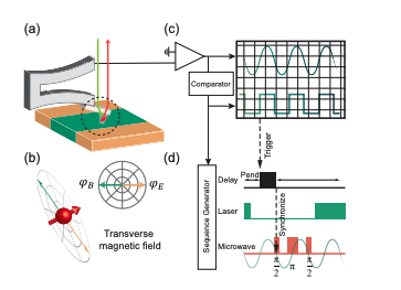
It addresses aspects not suitable for inclusion in the main text due to space constraints or complexity. Key sections detail time synchronization, simulation of spatial resolution, and probe design. The timing synchronization system coordinates the quantum control of the NV center with the mechanical oscillation of the probe, utilizing a quartz tuning fork for distance feedback. Spatial resolution was simulated using Fourier transforms to model electric field distribution and a 10%-90% edge width criterion. Probe design focused on balancing the tuning fork and minimizing off-axis oscillations with a counterweight and glass beam attachment.
Supplemental profile data obtained from imaging a defect provides wider and narrower field-of-view profiles. The technique relies on measuring the gradient of the electric field using the NV center, allowing for high-resolution imaging. Two modes of operation, intermittent-contact and shear-force, were implemented and compared. The sophisticated timing synchronization system is critical for achieving accurate measurements, and the careful design of the probe is essential for minimizing noise and maximizing stability. Simulations allow for a thorough understanding of the spatial resolution of the technique. Detailed explanations, clear organization, visual aids, transparency, and anticipation of potential questions are strengths of the supplementary materials. Future work may focus on providing more detailed simulation parameters, performing error analysis, and describing calibration procedures.
Nanoscale Electric Field Imaging with NV Centers
Scanning nitrogen-vacancy (NV) center electrometry now achieves an enhanced spatial resolution of approximately 10 nanometers, representing a significant advance in nanoscale electric field imaging. Researchers developed an axially symmetric probe with a sub-nanometer oscillating amplitude, enabling robust intermittent-contact mode feedback and close engagement between the diamond tip and the sample surface. This innovative approach simultaneously maximizes sensitivity and minimizes interference, delivering unprecedented resolution. Experiments demonstrate the protocol’s capabilities on ferroelectric lithium niobate, successfully resolving nanoscale polar textures and dynamics.
The team acquired an electric field gradient map over an 18 micrometer area, revealing a series of periodic stripes with a periodicity of 10 micrometers, consistent with piezoresponse force microscopy measurements. Detailed analysis of domain walls showed a 10%-90% edge-width criterion yielding a spatial resolution of approximately 10 nanometers. Validation of the electrometry protocol involved applying a static electric field, and the measured data perfectly matched theoretical predictions. Fitting the experimental data yielded effective electric fields of 2. 36 kilovolts per centimeter and 2. 61 kilovolts per centimeter, confirming the accuracy of the technique. This breakthrough delivers the ability to directly resolve features on the scale of tens of nanometers, opening new avenues for materials science and nanotechnology.
Nanoscale Electrometry with Diamond NV Centers
Researchers have developed a new scanning protocol using nitrogen-vacancy (NV) centers to achieve enhanced spatial resolution in electrometry, reaching approximately 10 nanometers. This advancement addresses a key limitation in nanoscale electric field imaging, where achieving high resolution is often compromised by electrostatic screening and signal averaging. The team accomplished this by designing an axially symmetric probe with a sub-nanometer oscillating amplitude, enabling robust intermittent-contact mode feedback and close engagement between the diamond tip and the sample surface. This innovative approach was experimentally demonstrated on lithium niobate, a ferroelectric material exhibiting nanoscale polar textures and dynamics.
The achieved 10-nanometer resolution allows for the direct observation of these features, which typically occur on scales of tens of nanometers. The researchers acknowledge that directly comparing the resolution of intermittent-contact and shear-force modes is challenging due to differing definitions used in their analysis. Future work may focus on refining these comparative metrics and exploring the full potential of this technique across a wider range of materials and applications. This breakthrough promises.
🗞 High-resolution electric field imaging based on intermittent-contact mode scanning NV center electrometry
🧠 ArXiv: https://arxiv.org/abs/2509.11586


