The drive to create ever-smaller and more efficient electronic devices focuses attention on the behaviour of materials as they transition between conducting and insulating states, a phenomenon central to modern information technology. Nicolò D’Anna from the Paul Scherrer Institute, Jamie Bragg from the London Centre for Nanotechnology, and Aidan G. McConnell, also from the Paul Scherrer Institute, and colleagues, have investigated these transitions in ultra-thin layers of silicon doped with arsenic and phosphorus. Their research demonstrates that, as the material approaches an insulating state, interactions between electrons become dominant, exceeding the effects of electron movement within the material. This finding challenges conventional understanding of these transitions and suggests that the behaviour of electrons near a metal-to-insulator transition is more complex than previously thought, potentially influencing the design of future nanoscale electronic components.
Silicon lies at the core of modern information technology because it easily switches from an insulator to a metal via either chemical doping or electrical gating. This unique property underpins the functionality of transistors and integrated circuits, driving the continued miniaturisation of electronic devices. However, further scaling faces significant challenges, including increased power dissipation and limitations imposed by conventional materials. Researchers therefore explore alternative materials and device concepts to overcome these hurdles and maintain the pace of innovation in the field. This work investigates the potential of two-dimensional silicon, specifically silene and silicene nanostructures, as promising candidates for future electronic devices, offering enhanced performance and reduced power consumption compared to bulk silicon. The research focuses on understanding the electronic and structural properties of these materials, and on developing methods to control their behaviour at the nanoscale, ultimately aiming to realise novel electronic components with improved characteristics
Delta-Doped Silicon Layers Characterization and Fabrication
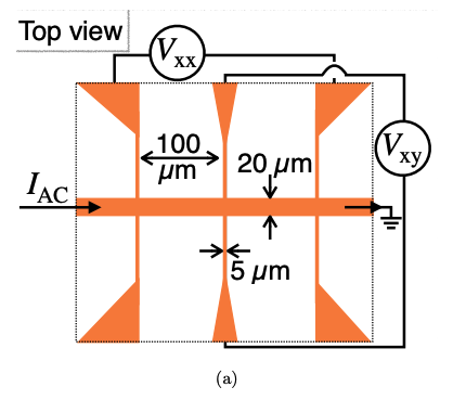
This supplemental information details experimental work on silicon layers containing extremely thin regions with a high concentration of added atoms, known as delta-doped layers, likely for use in advanced quantum devices. The research focuses on understanding how electrons move through these layers, particularly how factors like density and imperfections influence their behaviour. The team fabricated ten silicon samples, each with varying concentrations of arsenic or phosphorus incorporated as dopants, meticulously controlling the fabrication process to create high-quality delta-layers and thoroughly characterising their electrical properties at very low temperatures. Detailed characteristics of each sample, including the depth of the doped layer, electron density, mobility, and conductivity, are presented and analysed.
These measurements allow researchers to distinguish between effects related to the concentration of electrons and those linked to their energy. The data reveals that both arsenic and phosphorus behave similarly as dopants, suggesting the dopant type isn’t a major factor in the observed effects. The team employed specific analytical techniques to account for various factors influencing the measurements, ensuring accurate interpretation of the results.
Dopant Control Reveals Insulator Transition in Silicon
Silicon remains central to modern technology, and researchers continue to explore its potential for advanced computing by studying how it transitions between conducting and insulating states. Recent advances in creating extremely thin layers of dopants have allowed scientists to recreate a specific theoretical model of this behaviour, known as the two-dimensional disordered Hubbard model. By carefully controlling the distance between these dopant atoms, researchers have been able to observe the transition from a conducting to an insulating state in unprecedented detail. The team created layers of arsenic and phosphorus, just fractions of a nanometer thick and incredibly dilute, within silicon.
As the material approached an insulating state, they discovered that conventional explanations for changes in conductivity, based on the orbital motion of electrons, were overtaken by interactions between the electrons themselves. These interactions, governed by a predictable scaling law, actually reduced the flow of electricity, a surprising result that rules out some previously proposed explanations for this behaviour. Crucially, the researchers were able to isolate and measure the impact of these electron-electron interactions, revealing a logarithmic relationship with a combined measure of magnetic field and temperature. This allowed them to collapse data collected at various temperatures onto a single curve, demonstrating a fundamental underlying principle at play. This level of control and observation has not been achieved in these types of silicon layers before, and provides a new understanding of how electrons interact in these materials. Furthermore, the team found that the thickness of these dopant layers directly impacts conductivity; in the thinnest layers, conductivity is limited to just a few conductive planes within the silicon, compared to thirteen in thicker layers.
Electron Interactions Dominate Ultra-Thin Layer Conductivity
Magneto-transport measurements on ultra-thin layers of arsenic and phosphorus within silicon demonstrate that conventional models of conductivity, based solely on weak localisation effects, are insufficient to explain the behaviour of these materials. The research reveals significant contributions from electron-electron interactions, which become dominant as the layers become thinner and less densely doped. These interactions diminish conductivity through a mechanism linked to Zeeman splitting, an effect related to the magnetic properties of electrons, and combine with weak localisation in an additive manner. The findings confirm that the observed effects are independent of the dopant species, arsenic or phosphorus, and that spin-orbit coupling plays a negligible role in magneto-conductance. This suggests that the observed changes in conductivity are primarily driven by the interactions between electrons, rather than their spin. While the study successfully incorporates electron-electron interactions into the description of conductivity in these systems, the authors acknowledge that the precise nature of these interactions requires further investigation.
🗞 Strong electron-electron interactions in a dilute weakly-localized metal near a metal-to-insulator transition
🧠 ArXiv: https://arxiv.org/abs/2508.02793


