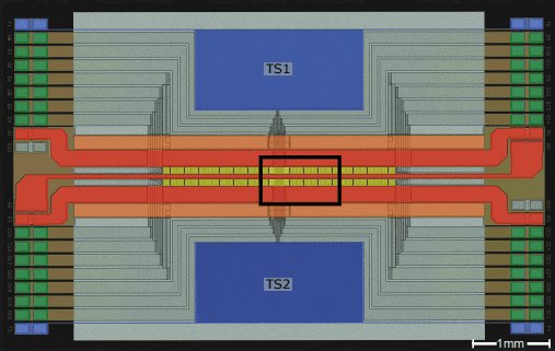
A multi-metal layer ion trap fabricated on fused silica demonstrates reduced power dissipation and improved performance compared to silicon-based designs. Integrated temperature sensors function at 10 K, and automated wafer testing validates each chip. Characterisation using a single trapped ion confirms lower electric field noise and stray fields.
The development of scalable ion trap technology represents a significant pathway towards realising a functional quantum computer. Addressing limitations in current fabrication methods, particularly those relating to power dissipation and manufacturing quality, is crucial for increasing the complexity of these devices. Researchers from Infineon Technologies Austria AG, the University of Innsbruck, the University of Graz, and the Austrian Academy of Sciences, alongside Alpine Quantum Technologies GmbH, detail their work on a novel multilayer ion trap fabricated on a fused silica substrate in their paper, ‘Test and characterization of multilayer ion traps on fused silica’. The collaborative team, comprising M. Dietl, M. Valentini, F. Anmasser, A. Zesar, S. Auchter, M. van Mourik, T. Monz, R. Blatt, C. Rössler, and P. Schindler, present a design and fabrication process that minimises power consumption and incorporates automated wafer testing, demonstrating improved performance compared to silicon-based traps. Their work focuses on characterising the electrical properties of the trap, including temperature sensing down to 10 K and the measurement of electric field noise using a single trapped ion as a sensitive probe.
Fused Silica Ion Traps: Advancing Scalable Quantum Computing
Quantum computing holds the potential to revolutionise computation across numerous disciplines, but realising practical quantum computers necessitates overcoming substantial engineering hurdles. Ion trap technology confines individual ions – electrically charged atoms – using electromagnetic fields, utilising their quantum states as qubits, the fundamental units of quantum information. Recent advances detail the fabrication and characterization of a multi-layer ion trap constructed from fused silica, demonstrating improvements in performance and scalability compared to conventional silicon-based designs. This approach directly addresses limitations inherent in traditional fabrication methods and facilitates the development of more complex and reliable quantum processors.
A primary obstacle to scaling ion trap systems lies in the complexity of fabrication and control, requiring precise manipulation of electromagnetic fields within ultra-high vacuum environments. Traditional traps, often etched into silicon substrates, suffer from material limitations that contribute to power dissipation and increased electric field noise, ultimately degrading qubit coherence – the duration for which a qubit maintains its quantum state – and limiting the fidelity of quantum operations.
Researchers have addressed these issues by fabricating a multi-layer ion trap on a fused silica substrate, departing from conventional silicon-based designs. Fused silica, a form of glass, exhibits significantly lower dielectric loss than silicon, substantially reducing power dissipation and improving overall system efficiency. The trap’s multi-layer design, created using photolithography and etching techniques, allows for complex electrode geometries necessary for precise ion confinement and manipulation, enabling greater control over qubit interactions.
Maintaining stable and precise control over the ion’s environment is critical for preserving qubit coherence, demanding meticulous attention to temperature control and minimization of external disturbances. The fabricated trap incorporates integrated temperature sensors directly onto the substrate, enabling accurate monitoring and control of the cryogenic environment essential for minimizing thermal noise and maintaining qubit stability. Cryogenics are required to reduce the motion of the ions, and thus reduce errors.
A significant innovation lies in the implementation of automated wafer testing, streamlining the fabrication process and ensuring the reliability of the fabricated devices. This testing occurs before assembly, establishing a robust platform for future development and experimentation.
The electric field within the trap is optimized through extensive simulations and experimental measurements to fine-tune the trapping parameters. This optimization ensures the integrity of the qubit.
These results represent a substantial step towards building larger, more stable, and more scalable ion trap quantum computers, demonstrating the potential of fused silica as a promising material for future quantum processors. Further research will likely focus on increasing trap complexity and ion number while maintaining the demonstrated levels of performance and reliability.
Researchers are actively exploring techniques for scaling up the fabrication process, including the development of advanced lithography techniques and automated assembly methods. They are also investigating new electrode designs and control schemes to further improve the performance and stability of the traps. The ultimate goal is to create a modular and scalable quantum processor that can be used to solve complex problems in various fields, including materials science, drug discovery, and financial modeling.
The development of robust and reliable quantum computers requires a multidisciplinary approach, bringing together experts in physics, engineering, materials science, and computer science. Collaboration between research institutions and industry partners is essential for accelerating the development and deployment of this transformative technology.
The integration of classical control systems with the quantum processor is another critical area of research. Developing efficient and reliable control algorithms is essential for manipulating the qubits and performing complex quantum computations.
The long-term stability and reliability of the quantum processor are paramount for practical applications. Researchers are investigating various techniques for mitigating the effects of environmental noise and imperfections, including shielding the processor from electromagnetic interference and stabilizing the temperature.
The exploration of different ion species and trapping geometries is also an active area of research. Different ion species have different properties that may be advantageous for specific applications. Researchers are also investigating new trapping geometries to improve the scalability and performance of the quantum processor.
👉 More information
🗞 Test and characterization of multilayer ion traps on fused silica
🧠 DOI: https://doi.org/10.48550/arXiv.2505.21284


