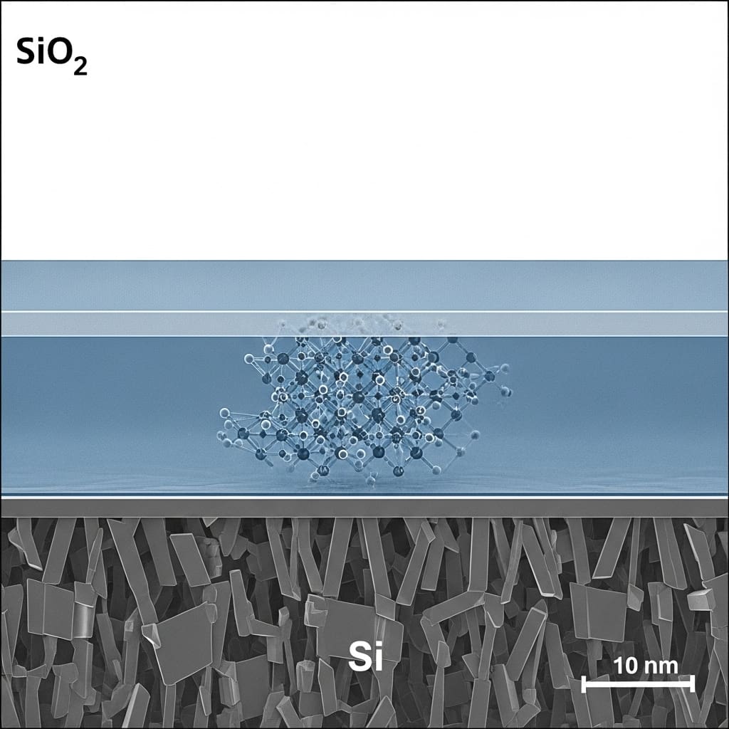
Precise placement of individual dopants within silicon is crucial for developing the next generation of electronic devices, and researchers are now achieving unprecedented control over this process. Ella B Schneider, Oscar G Lloyd-Willard, and colleagues at the University of Surrey, alongside Kristian Stockbridge from Ionoptika Ltd., demonstrate a highly efficient method for detecting single ion implants using secondary electrons within a focused ion beam system. This non-destructive technique achieves up to 98% detection efficiency, verified through careful calibration, and offers approximately 30 nanometre spatial resolution without the need for electrical contacts or complex device fabrication. Importantly, the team finds that a thin layer of silicon dioxide dramatically improves signal detection, paving the way for robust and scalable donor placement strategies applicable to a wide range of materials and device designs.
This breakthrough relies on measuring secondary electrons emitted when ions impact the silicon surface, and significantly enhances detection by introducing a thin layer of silicon dioxide on the material’s surface. This technique is crucial for creating advanced nanotechnology, particularly quantum devices requiring atomic precision. Traditional methods for detecting single ions often lack the necessary sensitivity and spatial resolution. This new approach overcomes these limitations, enabling precise and reliable detection essential for deterministic doping, where dopant atoms are placed exactly where desired.
The team used a focused ion beam to deliver individual ions to the silicon surface and carefully calibrated the ion current to ensure each detected event corresponded to a single ion implantation. The key to this improved detection lies in the silicon dioxide layer, which enhances secondary electron emission. The layer increases the distance electrons travel before losing energy, and also makes it easier for these electrons to escape the surface. Researchers discovered an optimal thickness for the silicon dioxide layer, maximizing detection efficiency while maintaining a high probability of ion implantation into the silicon.
The method proves robust, tolerating variations in layer thickness for different ion energies. Theoretical analysis, including the Lindhard-Scharff theory, explains the observed trends. This theory describes how ions lose energy as they travel through a material, and aligns with the observed decrease in detection efficiency with increasing atomic mass of the implanted ion. The increased inelastic mean free path within the silicon dioxide layer is a crucial factor in enhancing secondary electron emission. This research builds upon previous studies of secondary electron emission from both silicon dioxide and silicon, offering a significant advancement in the field.
This successful demonstration opens doors for significant applications in deterministic doping, quantum device fabrication, and other areas of nanotechnology. Future research will focus on optimizing the silicon dioxide layer for different ion species and energies, exploring alternative materials for enhancing secondary electron emission, and developing even more sensitive detection systems. Removing the silicon dioxide layer after implantation to reveal the implanted dopant is another avenue for future investigation.
Real-time Single Ion Detection by Secondary Electrons
Scientists have achieved highly sensitive, real-time detection of individual ion implantation events using secondary electrons, achieving up to 98% single-ion detection efficiency. This offers a non-destructive method for precisely locating dopants without requiring electrical contacts or pre-fabricated devices. The team implanted low-energy antimony ions into silicon and meticulously calibrated the ion current to quantify detection efficiency with high precision. To enhance the signal, researchers introduced a controlled silicon dioxide capping layer, finding it significantly increased secondary electron yield.
This improvement stems from the increased electron mean free path within the oxide compared to silicon, facilitating greater escape probability of emitted electrons. They determined the optimal oxide thickness to maximize both implant success and detection efficiency, carefully balancing signal enhancement with maintaining a high probability of ion deposition. Experiments achieved approximately 30nm spatial resolution, and the method is compatible with a broad range of host materials, including diamond and silicon carbide. Researchers investigated the relationship between ion velocity and detection efficiency, discovering that heavier ions require increased energy to maintain comparable detection rates.
This understanding, coupled with analysis of the Lindhard-Scharff electronic stopping model, explains species and energy trends in terms of changes in escape probability and inelastic mean free path. This technique provides a robust and scalable route for deterministic single-ion implantation, enabling non-destructive integration of donor-based quantum devices and colour centres across diverse material platforms. The ability to detect each implantation event in real time allows the beam to terminate upon successful arrival of a single ion, ensuring precise placement and minimizing errors.
Single Ion Detection Enables Precise Silicon Doping
Scientists have achieved a breakthrough in deterministic donor placement in silicon, essential for scalable devices, by developing a highly efficient method for detecting individual ion implantation events, achieving up to 98% detection efficiency. This relies on measuring secondary electrons generated within a focused ion beam system and offers a non-destructive approach to precisely locate dopants without requiring electrical contacts or pre-fabricated devices. Researchers found that introducing a controlled silicon dioxide capping layer substantially enhances secondary electron yield, consistent with an increased electron mean free path within the oxide, while simultaneously maintaining a high probability of successful ion deposition into the silicon substrate. They meticulously calibrated the ion current before and after implantation of arrays, measuring typical currents of 220fA, corresponding to one ion per pulse occurring every 727ns.
Analysis of the data involved extracting detection efficiency by accounting for factors such as blanker latency and dark counts, which were found to be several orders of magnitude smaller than the typical ion arrival rate. Linear regression performed on pulse duration and detected events yielded precise efficiency values, with standard deviations carefully quantified to ensure accuracy. The team demonstrated that the blanker latency remains consistent across different samples, suggesting an effective blanking region of approximately 10mm. Simulations using TRIM software confirmed the implanted ion depth profiles and frequency density, validating the experimental results and optimizing the silicon dioxide capping layer thickness for maximal implant success probability.
The optimal thickness range was determined to yield a total implant success probability within 99. 9% of its maximum value. This advancement enables precise dopant placement, paving the way for more sophisticated and scalable silicon-based devices.
Single Ion Detection via Focused Ion Beams
This research demonstrates a highly efficient method for detecting individual ion implantation events in silicon using focused ion beam microscopy and secondary electron detection, achieving up to 98% detection efficiency. This offers a non-destructive approach to precisely locate dopants without requiring electrical contacts or pre-fabricated devices. Researchers found that a thin capping layer of silicon dioxide enhances secondary electron yield, likely by increasing the mean free path of electrons within the oxide while maintaining successful ion deposition into the silicon substrate. The study establishes a clear relationship between ion velocity and detection efficiency, suggesting that heavier ions require increased energy to maintain comparable performance.
Analysis of the data supports the Lindhard-Scharff model for energy loss, showing consistency between experimental results and theoretical predictions regarding electronic stopping power. The team observed a slight decrease in detection efficiency with increasing atomic mass, aligning with the model’s expectations. Researchers acknowledge that the observed trends saturate at high yields, making precise quantification of secondary electron yield challenging. Further research could explore the limits of this technique with different materials and device architectures. This advancement provides a robust pathway for precise dopant placement, enabling the development of more sophisticated and scalable silicon-based devices.
👉 More information
🗞 Enhanced Secondary Electron Detection of Single Ion Implants in Silicon Through Thin SiO2 Layers
🧠 ArXiv: https://arxiv.org/abs/2510.14495


