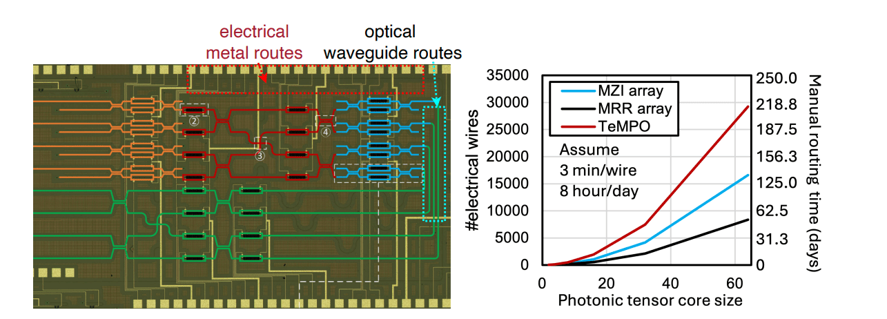
The increasing demand for artificial intelligence and scientific computing fuels the development of integrated photonic circuits, which offer significant advantages in speed and energy efficiency for data processing and communication. Hongjian Zhou, Haoyu Yang, Nicholas Gangi, and colleagues, present a new automated design framework that addresses a critical bottleneck in this field: the complex task of routing electrical connections within these increasingly intricate circuits. Their work introduces the first complete, end-to-end routing system that simultaneously manages both the optical waveguides and the metal wires that connect active components, a significant advancement over existing methods. By incorporating a physically-aware planning stage and optimised routing algorithms, the team achieves a dramatic reduction in design complexity, reducing the number of vias needed by approximately 99%, minimising design rule violations by 98%, and accelerating the routing process by a factor of 17 compared to manual design and conventional routing tools, paving the way for scalable electronic design automation of large-scale photonic integrated circuits.
Integrated photonics promises revolutionary advances in computing, sensing, and communications. As photonic integrated circuits (PICs) become more complex, designing them manually becomes increasingly impractical, necessitating a new era of electronic-photonic design automation (EPDA) where physical design, including the layout of optical waveguides and metal interconnects, can be fully automated. Current electronic design automation tools, however, are not directly applicable to PICs due to the unique constraints of photonic design.
Curvy Waveguide Routing for Photonic Circuits
Researchers have developed LiDAR, a new automated routing system designed to overcome the challenges of laying out large-scale PICs. A key difficulty lies in routing waveguides, often requiring curved paths for compact designs and efficient light management, something traditional routing algorithms struggle with. LiDAR specifically addresses this need by supporting curvy waveguide routing, automating the detailed layout process, and scaling to handle increasingly complex designs. The system recognizes that PIC routing differs significantly from conventional electronic circuit design, requiring strategies that account for the unique interactions between electronic and photonic components. Experiments demonstrate that LiDAR produces layouts with superior quality and improved scalability compared to existing methods, achieving a significant speedup in the routing process and reducing design time by up to 17x. This work establishes a foundation for scalable, fabrication-ready EPDA, accelerating the design cycle and enabling the creation of more complex and efficient photonic integrated circuits.
Photonic Integrated Circuit Routing With 99% Via Reduction
Scientists have created a complete end-to-end routing framework for large-scale active PICs, simultaneously optimizing both the layout of optical waveguides and the metal wires that connect the circuit’s components. This achievement overcomes the limitations of previous methods, which relied on manual scripting or were unsuitable for the specific demands of photonic design. The system employs a physically-aware global planner that generates routing guides, carefully considering component placement, waveguide layouts, and potential congestion. Experiments demonstrate a substantial reduction in the number of vias, the vertical connections between layers, achieving an average reduction of 99% compared to existing methods.
The new router also minimizes user-specified design rule violations, reducing them by 98%. Evaluations on various PIC designs, including complex circuits, consistently deliver high-quality solutions with fewer vias and lower congestion. On one benchmark circuit, the router achieved zero vias, used only one metal layer, and completed the routing in just 33 seconds. The team reports a 17x reduction in routing time compared to manual methods and existing tools, establishing a practical foundation for automated physical design at a system level.
Automated Layout Optimisation For Photonic Chips
Researchers have developed a new automated design framework that addresses a critical need in the development of large-scale active PICs. This is the first end-to-end routing solution capable of simultaneously optimizing both the waveguide and metal interconnect layouts, a significant advancement over existing methods. The framework integrates a photonics-aware global planner, a sequence-consistent track assignment method, and a detailed routing technique guided by “soft guidance” to achieve high-quality layouts. Evaluations on complex designs demonstrate substantial improvements over current approaches, including a 99% reduction in via count, a 98% decrease in design rule violations, and a 17-fold increase in routing speed.
These results establish a practical foundation for fully automated physical design automation at a system level, accelerating the design cycle and enabling the creation of more efficient and high-performance electronic-photonic systems. The researchers highlight that successful electrical routing for photonic circuits requires strategies distinct from those used in conventional microelectronics, acknowledging the unique interactions between electronic and photonic components. The researchers found that a “soft guidance” approach to routing effectively corrects deviations and maintains routing continuity, unlike “hard guidance”. This research lays the groundwork for scalable, fabrication-ready automation, paving the way for the next generation of manufacturable, energy-efficient, and high-performance electronic-photonic systems.
👉 More information
🗞 Photonics-Aware Planning-Guided Automated Electrical Routing for Large-Scale Active Photonic Integrated Circuits
🧠 ArXiv: https://arxiv.org/abs/2509.23764

