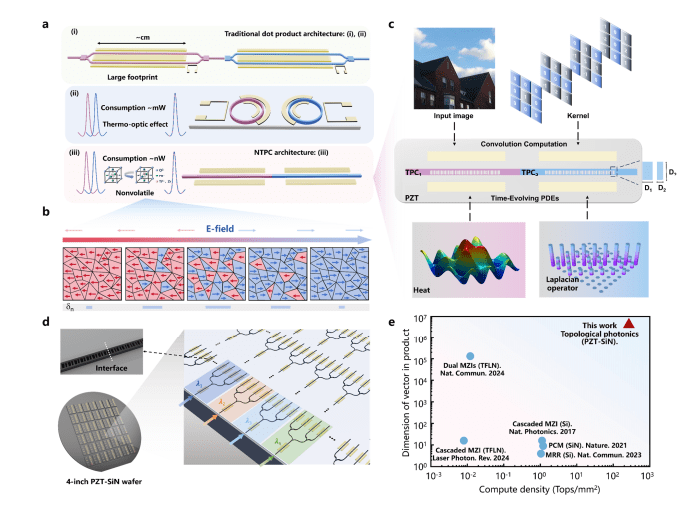
The relentless advance of artificial intelligence creates an ever-growing demand for faster and more efficient data processing, pushing the limits of current hardware. Wenfeng Zhou, Xin Wang, and Xun Zhang, along with their colleagues, address this challenge by unveiling a novel wafer-scale chip that harnesses the principles of topological photonics. Their research demonstrates a significant leap forward in processing speed and energy efficiency, achieving reconfiguration rates a thousand times faster than conventional silicon chips and operating with zero static power consumption. The chip delivers an impressive 266 trillion operations per second per square millimeter, vastly exceeding the capabilities of existing technologies, and establishes ferroelectric topological materials as a promising foundation for high-speed tensor processing and optical I/O.
PZT and Silicon Nitride Modulator Design
This research introduces a new integrated electro-optic modulator built on a combination of lead zirconate titanate (PZT) and silicon nitride (SiN). This innovative approach leverages the high efficiency of PZT in converting electrical signals to optical signals, combined with the stability and versatility of SiN for building photonic circuits. The modulator utilizes unique topological interface states within the PZT material, allowing for robust and efficient manipulation of light. By combining these materials, scientists have created a platform capable of high-speed light modulation for advanced applications.
The device demonstrates ultrafast coherent dynamics, enabling high-speed modulation crucial for next-generation communication and computing. This compatibility extends to Dense Wavelength Division Multiplexing (DWDM), a technology that significantly increases the capacity of optical communication systems. Furthermore, the technology enables high-fidelity matrix computation, essential for accelerating machine learning and artificial intelligence algorithms. This technology is well-suited for building photonic neural networks and other optical computing systems. Its high-speed and efficient matrix computation capabilities make it ideal for accelerating machine learning algorithms, while DWDM compatibility and high-speed modulation make it suitable for next-generation optical communication networks. The technology also promises to reduce energy consumption and increase bandwidth in data centers.
Wafer-Scale Topological Chip Fabrication and Design
Scientists have engineered a wafer-scale, non-volatile topological chip using ferroelectric lead zirconate titanate (PZT) thin films to address the growing demand for rapid and energy-efficient data processing. The fabrication process begins with depositing crack-free PZT films onto silicon dioxide substrates using a solution-based chemical deposition technique, ensuring compatibility with existing electronic technology and cost-effective manufacturing. To overcome challenges in etching thin PZT films, researchers implemented silicon nitride loaded PZT waveguides, capitalizing on established silicon nitride fabrication processes for large-scale integration. The chip design incorporates a 16-channel parallel processing architecture, achieved through a combination of wavelength-division multiplexing and spatial-division multiplexing.
Four front-end topological electro-optic modulators dynamically encode input data across four distinct wavelengths, while sixteen back-end modulators perform real-time weight updates across both wavelengths and spatial dimensions. These modulators utilize the high-speed Pockels effect in thin-film PZT, enabling rapid signal encoding and reconfiguration. Characterization of the fabricated topological cavity reveals a high quality factor and a significant extinction ratio, with a 3-dB splitter exhibiting minimal signal loss. To maximize modulation bandwidth and minimize footprint, the team optimized both material properties and structural innovation, leveraging PZT’s superior electro-optic coefficients and topological photonic crystal microcavities to achieve exceptional optical field confinement. The modulator operates via a topological interface state, rigorously maintaining single-mode operation and eliminating complex mode management.
Wafer-Scale Chip Achieves Record Computational Density
Researchers have developed a wafer-scale non-volatile topological photonic computing chip that delivers unprecedented computational density and speed. The chip is capable of performing 266 trillion operations per second per square millimeter, surpassing silicon reconfigurable chips by two orders of magnitude and thin-film lithium niobate platforms by four orders of magnitude. This breakthrough stems from the integration of topological modulators leveraging the GHz-speed electro-optic response and non-volatility of ferroelectric lead zirconate titanate (PZT) thin films. The 16-channel wavelength-space multiplexed chip achieves a throughput of 1.
92 TOPS, while maintaining high digit-recognition accuracy and precision when solving time-varying partial differential equations. Crucially, the chip operates with zero static power consumption, enabled by the intrinsic non-volatility of the PZT material, which allows for dynamic reconfiguration without sustained bias voltages. This non-volatility also facilitates functional reconfiguration for high bandwidth density optical input/output, achieving a shoreline bandwidth density exceeding 3. 56 Tbps per millimeter. Fabricated topological cavities exhibit a high quality factor and a significant extinction ratio, while a 3-dB splitter demonstrates minimal signal loss. The 4-inch PZT wafer fabrication technology supports further scalability through additional multiplexing dimensions, promising significantly enhanced on-chip computational capacity. This work establishes ferroelectric topological photonics as a powerful platform for efficient, high-speed tensor processing.
Ferroelectric Chip Achieves Record Computational Density
Researchers have successfully fabricated a wafer-scale chip leveraging ferroelectric topological modulators to achieve significant advances in high-speed, energy-efficient computing. The chip achieves a computational density of 266 trillion operations per second per square millimeter, exceeding the performance of both silicon reconfigurable chips and thin-film lithium niobate platforms by two to four orders of magnitude. The chip’s capabilities were validated through successful demonstrations in optical computing and optical interconnects, achieving high digit-recognition accuracy and precision when solving time-varying partial differential equations. Furthermore, the chip supports high-bandwidth density optical input/output. Scaling to larger modulator arrays and optimizing topology-specific algorithms will be crucial to fully realize the potential of this technology for applications in scientific computing and edge intelligence.
👉 More information
🗞 Ultrafast Reconfigurable Topological Photonic Processing Accelerator
🧠 ArXiv: https://arxiv.org/abs/2511.03432


