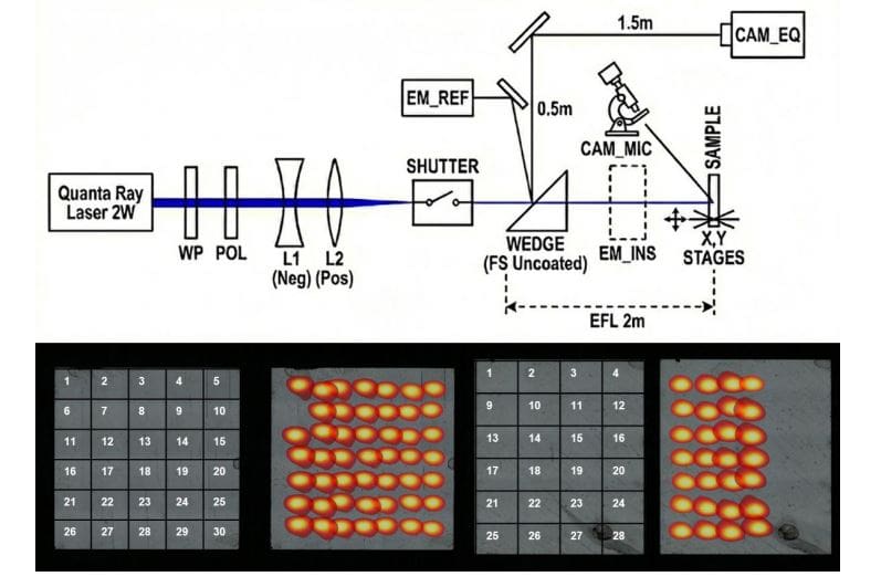
Defects in synthetic diamond severely limit its potential in advanced technologies, hindering performance in areas like high-power electronics and photonics. Adam H. Khan, Tae Sung Kim, and colleagues from Diamond Quanta and Lawrence Livermore National Laboratory demonstrate a method to significantly reduce these imperfections, achieving a breakthrough in diamond material science. The team employs nanosecond pulsed-laser induced densification to compact and reorganise damaged areas within single-crystal diamond, effectively relaxing strain associated with dislocations. Through detailed structural analysis, including interferometry and Raman spectroscopy, they reveal substantial reductions in surface defects and a measurable improvement in material uniformity to depths of several micrometres, paving the way for scalable production of high-performance diamond for a range of industrial applications.
Laser Smoothing Dramatically Reduces Diamond Defects
Scientists achieved significant smoothing and densification of diamond surfaces using nanosecond pulsed laser (PLA) processing, effectively reorganizing near-surface defect networks. Quantitative measurements, obtained through white-light interferometry, reveal substantial reductions in key surface parameters, including local slope, decreasing by 45 to 65 percent, and developed area, reduced by 60 to 90 percent. These changes correlate with a densification of approximately 4 to 6. 5 nanometers, indicating a compaction of the surface layer. Further analysis using depth-resolved Raman spectroscopy confirms relaxation of dislocation-mediated strain extending to depths of 2 to 3 micrometers, evidenced by narrowing of the diamond line and improved spectral uniformity.
Cross-sectional STEM imaging coupled with geometric phase analysis (GPA) provides direct visualization of smoother strain fields, suppressed hotspots, and redistribution of localized strain concentrations following PLA treatment. The data demonstrates a clear correlation between PLA processing and a reduction in the density of dislocations, which are known to limit device performance. These results establish that sub-melt PLA effectively compacts surface-connected free volume and reorganizes defect networks, leading to a measurable decrease in strain. The method offers a scalable approach for upgrading various industrial-grade diamond materials towards low-defect, device-ready surfaces, paving the way for improved performance in high-power electronics, photonics, and quantum technologies.
Laser Pulse Treatment Densifies Diamond Surfaces
This research demonstrates that nanosecond pulsed laser (PLA) treatment effectively reorganizes defects and reduces strain in the near-surface region of single-crystal diamond. By applying PLA, scientists achieved substantial reductions in surface roughness parameters, including slope, developed area, and height spread, alongside a significant decrease in void volume. These changes indicate a densification of the diamond surface, achieving compaction depths of approximately 4 to 6. 5 nanometers. Further analysis using Raman spectroscopy and strain mapping confirms that the benefits of PLA extend beyond simple geometric smoothing, revealing narrowing of the diamond Raman line and improved spectral uniformity to depths of up to 3 micrometers, indicating relaxation of strain associated with dislocations. Cross-sectional imaging revealed continuous crystalline diamond without the introduction of new defects, and strain maps showed smoother, lower-amplitude strain fields, suggesting redistribution of localized strain concentrations. This work offers a scalable pathway to improve the quality of diamond surfaces for applications in high-power electronics, photonics, and as substrates.
👉 More information
🗞 Reducing dislocation defect levels via sub-melt nanosecond pulsed-laser induced densification of diamond
🧠 ArXiv: https://arxiv.org/abs/2512.08719


