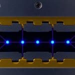
The pursuit of increasingly powerful quantum processors faces significant hurdles as qubit numbers grow, particularly concerning device consistency and seamless integration with control systems. Researchers led by Thomas H. Swift from Quantum Motion, alongside Alberto Gomez-Saiz and Virginia N. Ciriano-Tejel, address these challenges by developing a novel architecture for spin qubits in silicon. The team demonstrates the successful monolithic integration of 384 individual silicon dots, each functioning as a qubit, directly within a standard 22-nanometer silicon transistor chip. This innovative approach, which incorporates on-chip digital and analog electronics, allows for fast characterisation of qubit properties and reveals crucial links between device size, performance consistency, and noise levels, ultimately paving the way for scalable quantum computing systems built on established semiconductor manufacturing techniques.
Recent advances in quantum processors have created devices containing hundreds of qubits, the fundamental units of quantum information. As the number of qubits increases, significant challenges emerge, including reducing variations between qubits and integrating the necessary electronic control systems for input and output management. Spin qubits within silicon quantum dots offer a promising solution, demonstrating high control and readout accuracy and compatibility with established manufacturing techniques.
CMOS Quantum Dots at Cryogenic Temperatures
This research details the characterization of silicon quantum dots, tiny structures that confine single electrons, fabricated using standard CMOS technology at extremely low temperatures. The goal is to create a scalable platform for quantum computing using these dots. The team focused on the electrical properties of these devices, examining how they switch on and off, their inherent noise levels, and the impact of manufacturing variations. They also developed a method for accurately measuring the chip’s temperature at these cryogenic temperatures, addressing key challenges of scalability, control, and precise measurement.
The research emphasizes the use of standard CMOS fabrication processes, a major advantage for scalability as it leverages existing semiconductor manufacturing infrastructure. The devices operate at very low temperatures, around 4 Kelvin, to minimize thermal noise and enhance the stability of quantum states. The team investigated how the dots switch on and off, observing that the switching behavior is influenced by the device’s shape and manufacturing variations. A significant aspect of the work is the development of on-chip thermometers, built using CMOS technology, capable of accurately measuring temperature at cryogenic levels, essential for precise control and characterization. Ultimately, the goal is to create a scalable platform for quantum computing, requiring devices that can be fabricated in large numbers with consistent performance.
Dense Quantum Dot Array on Silicon Chip
Researchers have successfully integrated a remarkably dense array of 384 quantum dots onto a silicon chip, alongside conventional electronic control circuits, representing a significant step towards scalable quantum computing. The chip utilizes standard 22-nanometer manufacturing techniques, paving the way for compatibility with existing semiconductor industry infrastructure and potentially reducing production costs. The team meticulously characterized these quantum dots, extracting crucial parameters like size and electrical properties using automated, high-speed measurements at extremely low temperatures, around 600 millikelvin, essential for identifying and mitigating variations in qubit performance. Analysis reveals a clear relationship between the physical dimensions of the quantum dots and their electrical characteristics, allowing for better control and optimization of qubit properties.
The standard deviation of key parameters increases as the size of the quantum dots decreases, highlighting the challenges of manufacturing consistency at the nanoscale. Importantly, the researchers demonstrated that the performance of these quantum dots is not significantly affected by their location on the chip, a critical requirement for building large-scale quantum processors. The observed switching behavior demonstrates the viability of this approach for low-power operation. This monolithic integration, combining quantum and classical electronics on a single chip, offers a compelling solution to the challenges of managing input/output signals and qubit variability by minimizing signal delays and power consumption. The ability to rapidly characterize a large number of qubits on a single chip using automated techniques represents a major advancement in the field, accelerating the development of practical, scalable quantum computers.
Silicon Dot Integration and Scalable Quantum Control
This work demonstrates the monolithic integration of 384 silicon dots, each embedded within a transistor, alongside on-chip digital and analog electronics, all operating at deep cryogenic temperatures. Researchers successfully fabricated this chip using 22-nanometer fully-depleted silicon-on-insulator technology and developed automated routines to efficiently extract key parameters from the dots. Analysis of these parameters reveals a clear link between device dimensions and both the yield and variability of the dots, as well as the level of charge noise present, demonstrating a viable path towards scaling up the integration of quantum and classical electronics. Measurements of charge noise indicate values higher than those typically observed in other quantum platforms, highlighting the importance of addressing this issue for further development.
The team also characterized the impact of short-channel effects and manufacturing variability on device performance at these extremely low temperatures. Further research is needed to pinpoint the precise sources of variability and noise within the manufacturing process itself. This work provides an efficient method for extracting quantum dot parameters at scale and represents a significant advance in the field of cryogenic quantum electronics.
👉 More information
🗞 Large-scale characterization of Single-Hole Transistors in 22-nm FDSOI CMOS Technology
🧠 ArXiv: https://arxiv.org/abs/2507.21306


