Researchers are developing increasingly precise methods to control light at the nanoscale, a crucial step towards advanced photonic technologies and exploring fundamental light-matter interactions. Sergei Lepeshov from DTU, alongside Daniel Alec Farbowitz and Thor August Schimmell Weis, and their colleagues, now demonstrate a tunable silicon nanocavity capable of confining light to an exceptionally small volume. This innovative device employs nanoelectromechanical actuation, allowing for precise spectral control with minimal power consumption, and achieves theoretical performance metrics exceeding previous designs. The team’s work represents the first demonstration of a low-loss, tunable nanocavity of this type, paving the way for experiments in cavity electrodynamics and the development of scalable photonic systems that require strong light confinement and precise control.
Scientists present a new design for tunable nanocavities, fabricated from silicon, that efficiently trap and control light at the nanoscale. These structures enable strong interactions between light and matter, crucial for building advanced quantum photonic circuits. The research focuses on precisely controlling the nanocavity’s properties through nanoelectromechanical actuation, allowing dynamic adjustment of the light it traps without compromising its efficiency. This approach achieves spectral control over a broad range, while maintaining a high quality factor, representing a significant improvement over existing static designs. The work establishes a pathway towards scalable, dynamically reconfigurable quantum photonic integrated circuits for applications in quantum communication and computation.
Tunable Nanocavity Fabrication and Mechanical Control
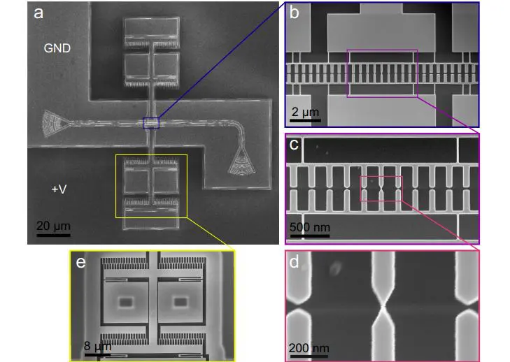
Scientists engineered a novel tunable nanocavity by integrating a silicon bowtie structure with nanoelectromechanical systems, achieving strong confinement of electromagnetic fields and compatibility with cryogenic environments. Fabrication involved electron-beam lithography, plasma dry etching, and selective underetching to create the intricate nanocavity structures. Researchers then coupled these cavities to photonic circuits and NEMS comb-drive actuators, enabling precise mechanical control. The team developed a method for simulating the deformation of the nanocavity under applied force, using this data to predict optical properties and calculate the spring constant associated with the cavity’s deformation.
Experiments employed comb drives to apply force, balancing electrostatic, spring, and deformation forces to determine cavity displacement as a function of voltage. Results demonstrate reversible tuning of the bowtie cavities across an 11nm spectral range, with a resonant wavelength sensitivity of 0. 23nm/V². The initial cavity exhibited a quality factor of approximately 18,000 and a normalized mode volume of 0. 2, yielding a Purcell factor of 6,600.
Importantly, the Purcell factor remained relatively stable across the tuning range, increasing slightly to 7,200 at 7V. Waveguide-coupling efficiency initially reached 30%, increasing to 40% at 6V due to enhanced mode confinement within the cavity’s squeezed air slot. Analysis of different mirror cell numbers revealed an optimal trade-off between quality factor and efficiency, with six unit cells providing the best performance.
Tunable Silicon Nanocavity Demonstrates Strong Coupling
Scientists have achieved a breakthrough in nanoscale photonics with the development of a tunable silicon nanocavity, demonstrating strong light-matter interactions and compatibility with cryogenic environments. This work delivers a low-loss dielectric nanocavity with a mode volume below 0. 2 cubic wavelengths, enabling theoretical Purcell factors exceeding 6,500 and waveguide-coupling efficiency above 30%. Crucially, the Purcell factor exhibits only weak dependence on the applied voltage, ensuring stable performance. The device utilizes nanoelectromechanical systems (NEMS) for tuning, employing comb-drive actuators to precisely control the air gap within the cavity.
Measurements confirm reversible tuning of the bowtie cavities, with the team directly observing in-plane actuation using in-situ characterization within a scanning electron microscope. Numerical analysis reveals that the fundamental electromagnetic mode exhibits strong electric field localization within the silicon bowtie and air slots, maximizing light confinement. Experiments demonstrate a spectral tuning range of 11nm, achieved through elastic deformation of the cavity structure. The design incorporates tapered-mirror sections and waveguide tapers to minimize mode mismatch and optimize coupling efficiency. This innovative approach overcomes a key limitation in cavity quantum electrodynamics, providing a cryocompatible tunable cavity concept for scalable photonic quantum technologies and enhanced experiments on strong light-matter interactions. The breakthrough paves the way for advancements in quantum light sources and silicon-based quantum photonics.
Tunable Silicon Nanocavities Demonstrate Strong Confinement
Researchers have successfully designed, fabricated, and tested tunable nanocavities based on silicon bowtie structures, demonstrating a significant advance in nanoscale photonics. These devices utilize nanoelectromechanical systems (NEMS) for tuning, offering compatibility with cryogenic environments and ultralow power consumption. The cavities achieve a mode volume below 0. 25 cubic wavelengths, coupled with a high quality factor, resulting in Purcell factors exceeding 1000. This strong light confinement and tunability address a key challenge in creating efficient platforms for exploring light-matter interactions and developing scalable photonic technologies. The team’s work represents the first demonstration of a low-loss, tunable dielectric nanocavity with strong light confinement, offering a pathway towards post-fabrication adjustment of single-photon sources and continuously tunable devices. Researchers acknowledge that future optimization may address slight deformation of the tuning mechanism, and suggest integrating quantum emitters into the center of the bowtie bridge could further enhance performance for applications in quantum photonics and quantum memories.
🗞 Nanoelectromechanical spectral control of silicon bowtie nanocavities for quantum light sources
🧠 ArXiv: https://arxiv.org/abs/2511.16153


