Understanding the behaviour of defects within two-dimensional materials is crucial for advancing nanoscale electronics, and a team led by Shubhrasish Mukherjee, Gaurab Samanta, and Shubhadip Moulick from S. N. Bose National Center for Basic Science now presents a significant step forward in this field. They investigate rhenium diselenide, a promising semiconductor, by creating devices with exceptionally clean interfaces, allowing them to directly observe the influence of individual defects. The researchers demonstrate that these defects, located within the hexagonal boron nitride supporting layer, cause random fluctuations in electrical current, and by carefully analysing these fluctuations, they identify carbon-related centres as the primary source of these imperfections. This work, which also includes contributions from Ruta Kulkarni at Tata Institute of Fundamental Research and Kenji Watanabe and Takashi Taniguchi at National Institute for Materials Science, establishes a powerful new method for characterising defects in advanced two-dimensional semiconductors and paves the way for more reliable and efficient nanoscale devices.
Rhenium Disulfide FET Noise Mechanisms and Analysis
Researchers investigated low-frequency noise in rhenium disulfide (ReS₂) field-effect transistors fabricated on hexagonal boron nitride (hBN). Detailed analysis of noise characteristics and calculations of key parameters, like trap density and the Hooge parameter, were performed on multiple devices to understand the underlying noise mechanisms and material properties. The study reveals that 1/f noise dominates, arising from carrier number fluctuations linked to interface trap density, ranging from approximately 4x 10¹¹ cm⁻² eV⁻¹ to 5x 10¹² cm⁻² eV⁻¹. This noise behaviour also demonstrates a dependence on the back gate voltage, supporting the carrier number fluctuation mechanism.
Data from multiple ReS₂ FETs consistently exhibit similar noise characteristics and follow the McWhorter model, strengthening the conclusions. The Hooge parameter, a measure of noise magnitude, yields comparable values to those reported for similar materials. This supplementary information provides a robust and detailed analysis of low-frequency noise, supporting the conclusion that carrier number fluctuations, governed by the McWhorter model, are the dominant noise mechanism.
Rhenium Diselenide Transistors on Hexagonal Boron Nitride
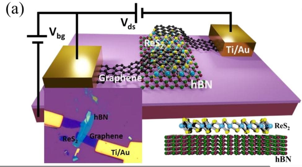
Researchers engineered a field-effect transistor platform using rhenium diselenide (ReS₂) as the channel material and few-layer graphene as electrodes, fabricated on a hexagonal boron nitride (hBN) substrate. This design overcomes limitations in observing intrinsic carrier dynamics in two-dimensional semiconductors by suppressing contact and disorder artifacts. The team mechanically exfoliated both the ReS₂ channel and graphene electrodes, carefully layering them onto the hBN substrate to create a clean interface crucial for minimizing extraneous noise and maximizing signal clarity. Transport and noise measurements were performed on multiple devices.
Raman spectroscopy confirmed the material’s structural integrity and crystalline quality. Room-temperature transport measurements verified linear current-voltage characteristics, indicating ohmic-like contact between graphene and ReS₂. Temperature-dependent transfer characteristics revealed n-type conduction with an excellent on/off ratio exceeding 10⁴ across all gate biases. Below 235 K, the device exhibited insulating behaviour, transitioning to mild metal-like behaviour at higher temperatures and gate voltages, demonstrating complex temperature-dependent charge carrier behaviour. Researchers extracted the subthreshold swing, achieving a value of 3.
5V/dec at room temperature, indicative of weak gate electrostatics and interfacial trap states. Field-effect mobility initially increased from 21 cm²V⁻¹s⁻¹ at 88 K to 30 cm²V⁻¹s⁻¹ at 130 K before decreasing with further temperature increases, explained by competing scattering mechanisms including Coulomb scattering and phonon interactions. To probe charge carrier dynamics, scientists employed a two-probe ac digital-signal-processing approach, revealing step-like features in drain current time series below 150 K, attributed to random capture and emission of charge carriers. Noise power spectral density analysis confirmed that the observed 1/f noise originated from intrinsic conductance fluctuations within the channel.
Defect Trapping Drives Current Fluctuations in ReS₂
This work demonstrates a platform for studying defects in two-dimensional materials, specifically rhenium diselenide (ReS₂) field-effect transistors, by integrating ReS₂ with hexagonal boron nitride (hBN) and employing graphene contacts. Researchers achieved nearly barrier-free interfaces, enabling observation of intrinsic transport properties and direct observation of random telegraph noise (RTN) even in micron-scale channels. Experiments revealed discrete two-level current fluctuations between 90 and 150 K, originating from stochastic trapping at localized defects within the hBN layer. The fabricated devices exhibit excellent on/off ratios exceeding 10⁴, with n-type conduction observed across all gate biases.
Below 235 K, the devices exhibited insulating behaviour, transitioning to mild metal-like behaviour at higher temperatures and gate voltages. Analysis of conductivity at different gate voltages showed that charge carrier activation primarily regulates electrical transport below 235 K. Field-effect mobility (μ) initially increased from 21 cm²V⁻¹s⁻¹ at 88 K to 30 cm²V⁻¹s⁻¹ at 130 K, followed by a decrease with further temperature increases. This behaviour is attributed to various scattering mechanisms, including Coulomb scattering and electron-phonon interactions. At temperatures exceeding 130 K, electron-phonon scattering dominates, with mobility scaling as μ ~ T⁻¹·³⁸.
At lower temperatures, charge impurities control electron transport, effectively increasing mobility. Low-frequency conductance fluctuations were studied using a two-probe ac digital-signal-processing approach, revealing random telegraph noise (RTN) and a transition from discrete fluctuations to a 1/f spectrum as temperature increased. Drain-current time series showed distinct step-like features below 150 K, attributed to random capture and emission of charge carriers at defect states. Statistical analysis identified substitutional carbon-related centres in hBN as the dominant defects responsible for these fluctuations. This work establishes a route to interrogate and engineer microscopic defect landscapes in 2D heterostructures for reliable, CMOS-compatible nanoelectronics.
👉 More information
🗞 Single-Defect Spectroscopy via Random Telegraph Noise in Graphene-Contacted ReS -hBN Heterostructures
🧠 ArXiv: https://arxiv.org/abs/2511.17125


