The pursuit of robust quantum technologies hinges on identifying materials that efficiently emit and control single photons, particularly within the wavelengths used for existing fibre optic networks. A team led by A. N. Anisimov, A. V. Mathews, and K. Mavridou are pioneering a new approach by engineering chlorine-vacancy defects within silicon carbide to achieve this goal. Their work demonstrates the creation and detailed characterisation of these colour centres, which emit light at key telecom wavelengths, spanning the O, S, and C bands. Crucially, the researchers confirm these defects arise specifically from chlorine incorporation into the silicon carbide, and they maintain strong emission even at very low temperatures, establishing them as a promising platform for building scalable, CMOS-compatible quantum networks.
Silicon Carbide for Quantum Light Sources
Research focuses on developing solid-state quantum emitters in silicon carbide (SiC) that operate at wavelengths ideal for quantum communication and technologies, particularly within the crucial 1. 5µm telecom band. SiC offers several advantages, including its mechanical and chemical robustness, scalability for large-scale fabrication, potential for integration with existing semiconductor technology, and the possibility of enhancing performance through isotopic purification. Scientists are investigating several types of point defects in SiC that exhibit quantum emission, including nitrogen-vacancy (NV) and vanadium (V) centers.
Vanadium centers are rapidly emerging as a leading contender, demonstrating emission within the telecom band, long spin coherence times, and controllable spin states. Researchers are also exploring divacancies and chlorine vacancies as potential emitters. A major goal is achieving emission in the 1. 5µm range for compatibility with existing fiber optic infrastructure. Controlling both the spin and optical properties of these defects is crucial for quantum information processing, and extending their coherence times is essential for building practical quantum devices.
Strategies to achieve this include using isotopically purified silicon, optimizing the defect environment, and operating at low temperatures. Researchers employ techniques like ion implantation, electron beam irradiation, and high-temperature annealing to create and control the density and distribution of defects, and are integrating these emitters with photonic waveguides to enhance emission rates. Isotopically enriched SiC is increasingly important for enhancing coherence, and waveguide integration and Purcell enhancement are key strategies for improving performance. Scientists are actively exploring new defect types and fabrication methods to further advance the field.
Creating ClV Centers in Silicon Carbide
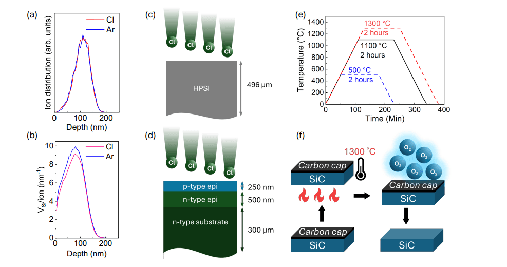
Scientists engineered chlorine-vacancy (ClV) color centers within silicon carbide to achieve emission in the crucial fiber-optic telecom bands. They pioneered a method involving chlorine ion implantation followed by high-temperature processing to deliberately create these defects within the crystal lattice, controlling the formation of vacancies paired with chlorine atoms. Researchers meticulously characterized the resulting ClV centers using photoluminescence spectroscopy, identifying four distinct configurations exhibiting sharp emission peaks at wavelengths spanning the O, S, and C bands. Controlled implantation experiments, varying chlorine concentration and annealing parameters, confirmed that the observed emission arises specifically from chlorine incorporation into the SiC structure.
The team harnessed computational tools to optimize the implantation parameters and predict chlorine distribution, ensuring precise control over defect creation. Further experiments demonstrated the high stability and coherence of the ClV centers, even at extremely low temperatures. Detailed spectral measurements revealed the distinct energy levels within the ClV defects, confirming their suitability for telecom-band applications. This work establishes ClV defects as a promising new class of color centers in a CMOS-compatible platform, offering strong potential for scalable quantum networks and advanced optical communication technologies.
Silicon Carbide Defects Emit Telecom Wavelengths
Scientists have experimentally realized and optically characterized chlorine-vacancy (ClV) color centers in silicon carbide, demonstrating emission within the crucial fiber-optic telecom bands, a significant step towards scalable quantum networks. The research team created these defects by implanting chlorine ions into silicon carbide followed by high-temperature processing, successfully generating four distinct ClV configurations. Photoluminescence spectroscopy revealed sharp emission peaks, or zero-phonon lines, located specifically within the O, S, and C bands, covering a broad range of telecom wavelengths. Controlled implantation and subsequent experiments definitively confirmed that the observed ClV centers originate from the incorporation of chlorine into the SiC material.
Optimization of the creation conditions resulted in stable, bright emitters across a wide range of the telecom spectrum. These findings establish ClV defects as a new class of telecom-band color centers within a CMOS-compatible platform, offering strong potential for building scalable quantum networks. Generating emitters directly within the standard telecom bands eliminates the need for complex and lossy frequency conversion techniques, paving the way for more efficient and practical quantum communication systems. This work demonstrates a pathway to integrate quantum technologies with existing fiber optic infrastructure, a crucial step towards realizing a quantum internet.
Chlorine Vacancy Centers Enable Telecom Wavelength Emission
Scientists have successfully created and characterized chlorine-vacancy (ClV) color centers within silicon carbide, demonstrating their potential for use in fiber-optic communication networks. These defects, generated through chlorine ion implantation and high-temperature processing, exhibit distinct optical properties, emitting light in the key O, S, and C telecom bands. The team confirmed that these ClV centers originate from the intentional incorporation of chlorine into the silicon carbide material. Researchers established conditions that maximize the strength of the emitted light signal relative to background noise, finding that a specific chlorine implantation fluence, combined with annealing at 1100 degrees Celsius, yields the highest signal quality.
Furthermore, the ClV centers demonstrate remarkable stability, maintaining strong emission even at extremely low temperatures. The formation of nitrogen-vacancy defects during the implantation process indicates a complex interplay of defect creation mechanisms. While further research is needed to isolate individual ClV defects, the demonstrated stability and spectral characteristics of these ClV centers represent a significant advance in the development of new materials for scalable, silicon carbide-based photonic technologies.
👉 More information
🗞 Engineering chlorine-based emitters in silicon carbide for telecom-band quantum technologies
🧠 ArXiv: https://arxiv.org/abs/2510.25008


